
A PCB design that performs its intended electrical functions is not necessarily ready for manufacturing and assembly.
Before sending Gerber files, the BOM, and other manufacturing data to a PCB assembly manufacturer, it is worth performing a pre-submission review. In addition to confirming that the bare board can be fabricated, check that the components, packages, assembly data, polarity information, test access, and file revisions are all consistent.
Many prototype projects require repeated engineering clarification not because the SMT process itself is especially difficult, but because the manufacturer discovers only after receiving the files that the BOM does not match the pick-and-place data, key components lack accurate manufacturer part numbers, DNP statuses conflict, or the PCB footprint does not match the package of the actual part being purchased.
If these issues are not discovered until quoting, component procurement, or production preparation, they can lead to additional clarification cycles, revised quotations, procurement delays, or design changes.
This article uses “PCB Assembly DFM Checklist” as a convenient general term. In practice, a pre-submission review often covers three related areas:
DFM (Design for Manufacturability) focuses on whether the PCB design and manufacturing data are suitable for consistent production.
DFA (Design for Assembly) focuses on whether the components, footprints, and layout are suitable for assembly, inspection, and any necessary rework.
DFT (Design for Testability) focuses on whether the completed assembly provides the access needed for programming, electrical testing, or functional verification.
For projects preparing to enter the prototype or NPI stage, reviewing all three areas together is more useful than checking only whether the Gerber files are sufficient to fabricate the bare board.
Start with a 5-Minute Pre-RFQ Quick Check
If you do not have time for a complete review, at least check the following items:
| Check Item | What to Confirm Before Sending the Files |
|---|---|
| Revision | Gerber files, BOM, pick-and-place data, and drawings all belong to the same build |
| PCB Requirements | Applicable requirements for board thickness, copper thickness, material, surface finish, stackup, and other parameters are defined |
| BOM | Key components include accurate manufacturer part numbers |
| Assembly Data | Pick-and-place data and assembly drawings are available |
| DNP / DNI | Assembly status is consistent across all documents |
| Footprints | The actual MPN, package, and PCB footprint match |
| Polarity | The orientation of polarized components is clearly defined |
| Testing | Programming, inspection, FCT, and other applicable requirements are broadly defined |
| Quantity | Prototype or pilot-build quantities are clear |
| Special Processes | Requirements for coating, press-fit parts, special cleaning, and other processes are documented |
This table does not replace a formal DFM review, but it can eliminate many common manufacturing-data problems before they reach the supplier.
1. Confirm That All Files Belong to the Same Build
One of the most underestimated issues during the prototype and NPI stages is revision control.
PCB designs often change quickly. The Gerber files may have been updated to Rev C, while the BOM used for purchasing is still Rev B and the pick-and-place file came from an even earlier CAD export.
Each file may appear correct when viewed separately. Together, however, they could produce a PCBA that was manufactured correctly according to the instructions, but built to the wrong revision.
Before sending the files, confirm that the Gerber files, BOM, pick-and-place data, assembly drawing, fabrication drawing, and any applicable firmware and test files all correspond to the same build.
For example:
Gerber = Rev C
BOM = Rev C
Pick-and-Place = Rev B
This should be resolved before the RFQ package is sent, rather than discovered when the assembly house begins creating the SMT program.
A prototype may not yet have a formally released production revision. What matters is that both sides clearly understand:
Which set of manufacturing data governs this build?
After a new revision is released, remove older files from the submission package or archive them clearly. Avoid sending the latest files together with obsolete versions in a way that could create ambiguity during engineering review.
2. Check Whether the PCB Fabrication Data Is Complete Enough
Having a complete set of Gerber files does not necessarily mean that all PCB manufacturing requirements have been clearly defined.
Gerber files primarily describe the graphical data for each layer. Actual fabrication usually also requires drill data, along with material, construction, tolerance, and other project-specific requirements.
Before sending the files, confirm that the board outline, layer count, NC drill data, finished board thickness, copper thickness, surface finish, stackup, controlled-impedance requirements, and any special via requirements have been defined.
For a conventional two- or four-layer FR-4 prototype, the fabrication requirements may be relatively straightforward.
If the project involves HDI, blind or buried vias, rigid-flex construction, controlled impedance, special materials, heavy copper, or tight mechanical tolerances, Gerber files alone may not fully communicate the design intent. In such cases, a fabrication drawing, stackup, or project specification is usually also required.
For example, if a design requires controlled impedance but does not specify the target impedance or the corresponding stackup conditions, the PCB manufacturer cannot determine the required construction from the copper artwork alone.
If the project uses an integrated manufacturing-data format such as ODB++, some graphical, drill, and net information may already be included in the package. The final RFQ package should still be prepared according to the specific supplier’s requirements.
The goal is not to provide as many files as possible. The goal is to ensure that the manufacturer does not have to guess about critical PCB requirements.
3. Check the Board Edge, Panelization, and Depanelization Impact
Some layouts pass all CAD design-rule checks but reveal mechanical problems during assembly or depanelization.
Components placed too close to the board edge are a common example.
It is not appropriate to define one universal rule stating that every component must be at least X mm from the board edge. The required clearance depends on the PCB thickness, component size and height, panel design, V-scoring or routing method, fixture support, and depanelization equipment.
Before sending the files, a more practical review is to check whether components extend into the intended depanelization area, whether connectors require a specific board-edge overhang, whether tooling rails need to be reserved, and whether depanelization could apply excessive mechanical stress to nearby components.
Components that are sensitive to strain, such as ceramic capacitors, deserve particular attention when placed near panel breakaway areas.
Board-edge clearance is not only about whether the pick-and-place machine can place the component. It can also affect depanelization, inspection, rework, and subsequent mechanical assembly.
If panelization has a significant impact on the product structure or component placement, confirm it with the actual manufacturer before design freeze rather than waiting until all PCB files have been released.
4. Check Whether the Footprint Matches the Actual MPN
A correct MPN in the BOM does not prove that the PCB footprint is also correct.
This is one of the more costly types of errors during the prototype stage.
For critical components, check before submission that the manufacturer part number, package, pin count, pin 1 location, exposed pad, and PCB library footprint all correspond.
A single component family may include multiple body sizes, pitches, or exposed-pad configurations.
If the BOM specifies one QFN package while the layout library uses a different package from the same product family, the SMT process cannot compensate for this design-input error.
BGA, QFN, LGA, connectors, power components, and ICs available in multiple package variants should all be checked against the manufacturer’s package drawing and datasheet.
The recommended land pattern in the datasheet is usually an important starting point, but it should not be copied mechanically without considering the actual component and manufacturing conditions.
The final pad design may also be affected by solder-mask definition, via structure, thermal requirements, the assembly process, and the capabilities of the selected manufacturer.
For QFNs with exposed pads, do not assume that a fixed number of thermal vias is always required. Whether thermal vias are needed, and how the thermal path should be implemented, depends on the device power dissipation, PCB thermal design, and the manufacturer’s application guidance.
Before sending the files to the assembly house, resolve the most basic question:
Will the component being purchased according to the BOM actually fit and assemble correctly on the corresponding PCB footprint?
5. Component Spacing Is More Than Checking for Physical Collisions
Many PCB CAD tools check the geometric clearance between components.
However, “nothing overlaps” and “the design is suitable for production” are not the same thing.
For example, a fine-pitch IC may still be placeable even if it is surrounded tightly by tall components, while optical inspection or rework may become difficult.
Insufficient space around a connector can affect manual assembly, mating verification, or access for rework tools.
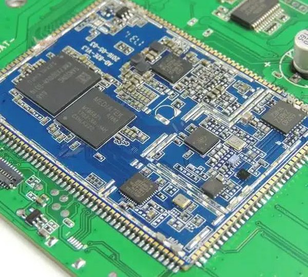
The placement of large or thermally massive components relative to nearby small components may also affect the local reflow-process window.
When reviewing component spacing, consider the full sequence:
Placement → Soldering → Inspection → Rework
If the components are near the board edge, include depanelization in the review as well.
There is no universal spacing value that applies to every package, SMT machine, and manufacturer.
A standard passive component, a fine-pitch QFN, and a large connector all require different considerations.
If the layout is already very dense, asking the actual assembly house to perform a DFA review based on its equipment and process capabilities is usually more effective than searching online for a single “minimum component spacing” value.
6. Review BGA, QFN, and Fine-Pitch Devices Together with the PCB and Assembly Process
The presence of a BGA or fine-pitch package does not automatically make a project high-risk or unusually difficult.
Manufacturing complexity is determined by how well the package size and pitch, pad design, via structure, PCB stackup, available routing space, and actual assembly process work together.
For example, BGA breakout may be handled with a conventional dog-bone fanout. In designs with higher routing density, smaller pitch, or insufficient escape space, via-in-pad or HDI microvias may also be considered.

However, via-in-pad should not be treated as the default solution simply because a BGA is present.
If conventional dog-bone routing can meet the design and layer-count requirements, introducing a more complex via-in-pad structure may only increase PCB fabrication cost.
When a via is located within an actual solderable pad, the appropriate via filling, capping or plating, and surface-flatness controls must be considered based on the fabrication structure. This helps prevent open vias from adversely affecting solder volume or joint formation. The specific via structure should be confirmed with the PCB manufacturer rather than assuming that all via-in-pad designs use the same process.
For QFNs with exposed pads, review the center pad, thermal design, via arrangement, and solder-paste strategy together.
A fixed thermal-via count or paste-coverage ratio should not be applied to every device. The component manufacturer’s guidance, power dissipation, thermal path, and assembly process all affect the final design.
For these packages, the better DFM question is not:
“Can you build BGA or QFN assemblies?”
It is:
“Are the current pad design, via structure, stackup, and assembly process compatible with this specific package?”
7. Remove Procurement Ambiguity Before Sending the BOM
A BOM suitable for quoting and production should allow the purchasing team to determine one thing clearly:
Exactly which component needs to be purchased.
For critical components, provide the complete manufacturer part number whenever possible. Also confirm that the reference designators, quantities, values, packages, and DNP / DNI statuses are accurate.
If substitutions are allowed, avoid writing only:
“or equivalent”
The boundaries of “equivalent” are not clear.
Similar electrical specifications do not necessarily mean that the package, temperature grade, lifecycle status, programming requirements, or project approval status are the same.
A clearer approach is to provide approved alternatives or an AVL, or to specify which components the supplier may substitute and which require customer approval.
For medical-electronics projects, substitutions of critical components may also affect risk management, design verification, and the customer’s own change-control process.
A supplier can help identify available purchasing options, but “available for purchase” and “approved for use in the design” are two different things.
8. A Pick-and-Place File Is More Than a Set of XY Coordinates
The pick-and-place file, also called a centroid file or CPL, is an important input for creating the SMT placement program.
Before sending it, confirm that the reference designators match the BOM, the top and bottom sides are clearly identified, the units and origin are correct, and the DNP / DNI status is consistent with the other manufacturing documents.
Rotation should also be reviewed, but it should not be used as the sole basis for determining polarity.
Different CAD tools, libraries, and export settings may use different zero-degree references and rotation conventions.
For directional components such as diodes, LEDs, ICs, and polarized capacitors, use the assembly drawing, datasheet, and clear pin-1 or polarity markings to communicate the intended orientation.
The main issue to avoid is this:
The BOM indicates one assembly status, the CPL indicates another, and the assembly drawing provides a third interpretation.
Once this conflict reaches production, the supplier can only pause the affected work and request clarification from the customer.
9. Use the Assembly Drawing to Communicate What Machine Data Cannot
If you already have Gerber files, a BOM, and pick-and-place data, why do you still need an assembly drawing?
Because machine data cannot fully communicate every aspect of the assembly intent.
Component polarity, connector orientation, DNP / DNI status, special hand assembly, mechanical hardware, labeling, coating keep-outs, and other assembly instructions may need to be documented in a drawing or project note.
A connector may have correct XY coordinates in the CPL, but the coordinates alone may not communicate the customer’s requirements for mechanical orientation, installation height, or assembly sequence.
The assembly drawing does not need to be overloaded with ordinary data.
Its purpose is to answer this question:
What important assembly information cannot be determined reliably from the BOM and placement data alone?
If the answer is “nothing,” the drawing can be simple.
If the project includes several special assembly conditions, those conditions should be documented clearly.
10. Consider Test Points and Programming Access During Layout
A PCB may be fabricated and assembled without difficulty, yet the NPI process can still be delayed if the finished assembly cannot be tested or programmed effectively.
This is where DFT becomes important.
If the project will use ICT, flying-probe testing, programming, or functional testing, consider the actual access requirements for testing and programming during the layout stage.
For example, programming pads may be blocked by tall components, fixture probes may not be able to reach test points, or the test interface may be too close to mechanical structures. Any of these issues can make fixture design more difficult.

Whether a large number of test points is necessary depends on the test strategy.
A prototype that only requires a basic power-on check has very different DFT requirements from a production project that will use automated ICT, programming, FCT, and serial-number-linked test-data recording.
If a dedicated fixture is already expected, have the test or manufacturing engineering team confirm probe access, interface locations, and mechanical clearances before layout freeze.
11. Define Testing Requirements Before the PCBA Is Built
Testing is often left until the end of the prototype RFQ process.
The customer may initially ask only:
“Please quote 50 pcs PCBA.”
After production is already underway, the customer may add programming, FCT, or calibration requirements.
The manufacturer then discovers that firmware, test procedures, fixtures, communication interfaces, or additional test equipment are required. Both cost and lead time may change as a result.
If the project requires programming, power-on testing, functional testing, calibration, or communication testing, provide the available test inputs during the RFQ stage.
These may include the firmware revision, input voltage, interface, main test procedure, pass/fail criteria, who is responsible for the fixture, and whether test data must be retained.
It may not be possible to define every test detail at the beginning of the project.
However, telling the manufacturer early what the product will ultimately need to verify is usually enough for it to assess whether fixtures, additional engineering work, or longer test time will be required.
12. Medical PCB Projects Require Clear Quality Requirements
The basic SMT process used for a medical PCBA does not automatically become a completely different manufacturing process simply because the final product is a medical device.
The more significant differences between projects usually come from quality requirements, traceability, inspection, testing, and documentation.
For example, a customer may require specific workmanship criteria, material traceability, serial numbers, inspection records, test records, or change approval.
The earlier these requirements are included in the RFQ and manufacturing package, the easier it is for the supplier to include the corresponding work in its quotation and scope.
A common misconception is:
Medical PCB = IPC Class 3 + 100% X-ray + ICT + FCT
That is not automatically true.
The medical application alone does not determine the applicable IPC class, nor does it automatically require every PCBA to undergo the same X-ray, ICT, or FCT scope.
If the project uses IPC-A-610, J-STD-001, or a customer-specific workmanship specification, clearly state the applicable class, revision, and any project-specific requirements.
ISO 13485 primarily addresses quality-management-system requirements for the medical-device industry. It does not replace a specific PCB assembly, inspection, or testing specification.
Instead of telling the supplier only:
“This is a medical project.”
It is more useful to specify:
What workmanship, inspection, testing, traceability, and documentation requirements actually apply to this project.
The 8 Most Common Issues That Can Put a Project on Hold
The following issues may appear minor, but if the manufacturer cannot determine which interpretation reflects the customer’s design intent, it may need to pause the project:
- Key components do not have complete MPNs in the BOM
- The Gerber files, BOM, and pick-and-place data belong to different revisions
- DNP / DNI status conflicts between documents
- The PCB footprint does not match the package of the actual MPN
- Polarity information for diodes, LEDs, ICs, or other directional components is unclear
- Critical PCB material, thickness, stackup, or surface-finish requirements are not defined
- Programming or testing requirements are missing
- New revisions are mixed with obsolete manufacturing files in the same RFQ package
These issues do not necessarily mean that the entire PCB design is wrong.
The problem is that the production team cannot reliably answer:
“Which data should we use to build this assembly?”
In such cases, the manufacturer should issue an engineering clarification request rather than make assumptions on the production line.
When Is It Worth Involving the Manufacturer Early in the DFM Process?
Not every conventional PCB requires frequent back-and-forth with the manufacturer from the early layout stage.
For a prototype with a conventional structure, mature packages, and sufficient design space, an internal review followed by a formal supplier DFM / DFA review is often sufficient.
However, early involvement from the actual manufacturing team becomes more valuable when the project includes HDI or microvias, fine-pitch BGAs, rigid-flex construction, very small components, special via structures, or complex SMT and through-hole assembly.
Complex testing is another clear signal.
If the project will require ICT, automated FCT, a programming fixture, calibration, or extensive test-data retention, DFT should not be considered only after the PCB layout has been completely frozen.
If a medical project already has detailed requirements for material traceability, serial-number tracking, or test records, it is also worth establishing the record-keeping approach during the prototype or NPI stage.
The purpose of early DFM involvement is not to have the supplier redesign the product. It is to identify issues related to actual manufacturing capabilities while design changes are still relatively easy to make.
The closer these issues are discovered to design freeze or tooling completion, the more difficult the changes usually become.
Final File Package for the PCB Assembly Manufacturer
After completing the pre-submission review, a typical PCBA RFQ package may include:
| File | Primary Purpose |
|---|---|
| Gerber files + NC drill, or an integrated manufacturing-data format accepted by the supplier | PCB fabrication |
| BOM | Component sourcing and assembly |
| Pick-and-place / centroid file | SMT placement |
| Assembly drawing | Assembly intent and special instructions |
| Fabrication drawing / stackup | PCB fabrication requirements |
| Programming files / instructions | Firmware programming, if applicable |
| Test specification | Inspection, electrical, or functional testing, if applicable |
| Revision note / file manifest | Identifies the data used for this build |
Not every project requires every file listed above.
A project that does not require programming does not need firmware files. A prototype that does not require functional testing does not need an FCT specification simply to make the package look complete.
What matters is this:
The submitted data must adequately describe the build, and the documents must not contradict one another.
Frequently Asked Questions
What is the difference between DFM and DFA?
DFM focuses primarily on whether the design and manufacturing data are suitable for consistent production. DFA focuses more specifically on whether the components, layout, and assembly requirements are suitable for assembly.
In PCBA projects, the two are often reviewed together.
For example, PCB via structures are more closely associated with DFM, while component spacing, polarity, and rework access are more closely associated with DFA. If the project also involves ICT, programming, or FCT, DFT should be considered as well.
Can a DFM review begin with only Gerber files and a BOM?
Yes, but only part of the review can be completed.
Gerber files and related PCB data can be used for a fabrication review, while the BOM can be used to begin component evaluation.
For a more complete PCB assembly review, you will usually also need pick-and-place data, an assembly drawing, and any applicable programming and testing information.
Can the PCB manufacturer directly fix DFM issues?
The manufacturer can propose DFM improvements.
If the change involves internal panelization or production preparation that does not alter the customer’s design intent, it can often be handled according to the agreement between both parties.
If the change affects customer-defined traces, pads, vias, footprints, components, or other design elements, customer approval should be obtained before implementation.
How much spacing should be left between components?
There is no single value that applies to every package, PCB, and SMT manufacturer.
The decision should consider component size and height, placement equipment, soldering, inspection, rework, depanelization, and the capabilities of the actual factory.
When the layout is dense, having the target assembly house review the specific layout is generally more reliable than applying a generic spacing value.
Does a medical PCB always require IPC Class 3?
No.
The medical application alone does not automatically determine the required IPC class.
The applicable class, workmanship, inspection, and test scope should be defined according to the product requirements, customer specifications, and the agreed purchasing and manufacturing documents.
When is the best time to perform a PCB assembly DFM review?
The earlier a manufacturing issue is identified, the easier it usually is to adjust the design.
For a conventional prototype, complete a DFM / DFA review at least before manufacturing release.
For projects involving HDI, fine-pitch BGAs, rigid-flex construction, special materials, complex testing, or strict medical traceability requirements, it is better to involve the manufacturer in key reviews before the layout reaches design freeze.
Final Check Before Sending the Files
PCB assembly DFM should not answer only one question:
“Can this PCB be built?”
Before entering the prototype stage, also confirm that the PCB fabrication requirements are clear, the BOM can be purchased accurately, the footprints match the actual components, the pick-and-place data and assembly drawing are consistent, polarity is unambiguous, and programming and testing have been considered.
Then perform one final check:
Do all of these documents describe the same build?
If these issues are resolved before the RFQ is sent, the manufacturer can usually reduce unnecessary engineering back-and-forth and provide a more accurate assessment of cost, lead time, and production-preparation requirements.
If the project is still in the NPI stage, there is no need to delay the first DFM discussion until every detail is completely frozen.
For projects involving HDI, fine-pitch packages, rigid-flex construction, special assembly, or complex testing, involving the manufacturing team while the design can still be adjusted is usually more effective than addressing all issues after the layout is complete.
Send Your Gerber, BOM, and Assembly Files for DFM Review