
Conventional through-via multilayer construction can become impractical when fine-pitch packages and limited board area leave too little room for escape routing. High-Density Interconnect, or HDI, increases routing density through microvias, finer conductor geometry, via-in-pad structures, and build-up layers.
HDI does not automatically mean a board is better, more reliable, or more advanced. It is a construction approach used when package geometry, interconnect density, or product dimensions make a conventional multilayer PCB difficult to route. This article explains how HDI boards are structured, how they differ from standard multilayer PCBs, and when the added manufacturing complexity is justified.
Table of Contents
What Makes a PCB an HDI PCB?
HDI describes a PCB with a higher interconnection density per unit area than a conventional board. This density is usually achieved through a combination of microvias, small capture pads, fine conductor geometries, via-in-pad processing, and build-up construction.
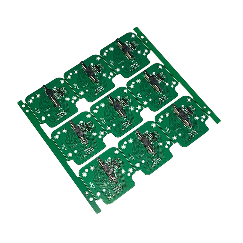
Industry references associated with IPC-2226 often describe HDI features using conductor widths and spaces around or below 100 μm, microvias around or below 150 μm, and small capture pads. These values are useful indicators of high-density construction, but they should not be treated as universal pass-or-fail limits for every HDI design.
Current IPC terminology places more emphasis on microvia structure. A microvia is generally a blind, shallow interconnect with a maximum depth-to-diameter ratio of 1:1 and a total depth no greater than 0.25 mm. Many PCB fabricators apply tighter preferred limits to improve production robustness.
Common interconnect structures
Microvias are usually laser-formed blind vias that cross one thin dielectric layer between adjacent copper layers. Connections across additional build-up layers are created with stacked or staggered microvia structures.
Blind vias connect an outer layer to one or more inner layers without passing through the full board. Buried vias connect inner layers only. Via-in-pad places the via directly within a component pad and is often used when conventional fan-out does not fit beneath a fine-pitch BGA or CSP.
HDI does not necessarily replace every through via. Many HDI boards combine plated through-holes, buried vias, blind microvias, and via-in-pad structures according to the routing and assembly requirements.
IPC HDI construction types
IPC-2226 describes several HDI construction types based on the number of microvia layers and whether buried vias are present.
- Type I uses a single microvia layer on one or both sides of the core without buried vias in the central core.
- Type II uses a single microvia layer and adds buried vias within the core.
- Type III uses two or more microvia layers on one or both sides and may also include buried vias.
Practical stack-up notation such as 1+N+1 and 2+N+2 describes the number of build-up layers around a conventional central core. These notations are useful for discussing construction, but they should not be treated as direct substitutes for IPC Type I, II, and III.
Any-layer HDI is a more advanced structure in which laser-drilled interconnections can be formed between many or all layer pairs. It should not be treated as another name for IPC Type III.
A board is therefore not HDI simply because it has many layers or a small outline. An eight-layer board using only conventional through vias may not be HDI, while a lower-layer-count board using microvias and build-up interconnects may be.
How Does HDI Differ from a Standard Multilayer PCB?
The practical difference becomes clear when routing density increases.
In a conventional multilayer PCB, through vias extend through the full board thickness. Their pads and antipads consume space on every layer they cross, including layers where no electrical connection is made. This is usually acceptable on moderate-density designs, but it can restrict escape routing beneath high-ball-count BGAs and other fine-pitch packages.
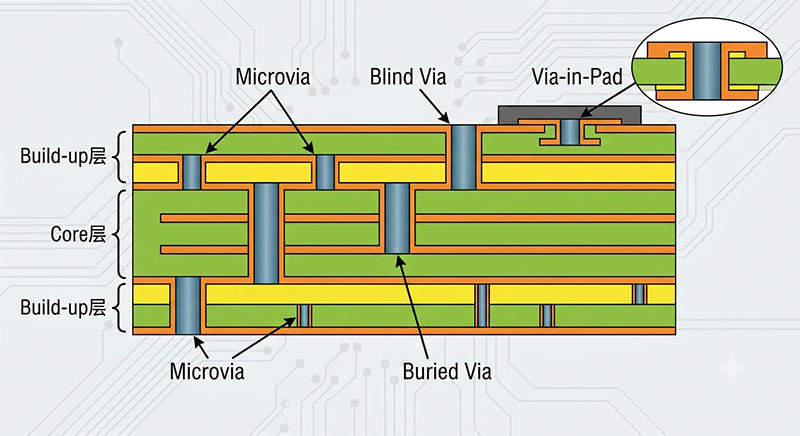
HDI places smaller interconnections only where they are needed. For example, an L1-to-L2 microvia uses no pad or antipad area on layers 3 through 8. This preserves inner-layer routing channels and can reduce the number of layers required to complete a dense fan-out.
| Design factor | Standard multilayer PCB | HDI PCB |
|---|---|---|
| Interconnect approach | Primarily through vias, with optional mechanically drilled blind or buried vias | Microvias and build-up interconnects used together with through, blind, or buried vias as required |
| Fine-pitch BGA escape | May become difficult at 0.5 mm pitch and below, depending on ball map and fabrication rules | Often supports more practical via-in-pad and microvia fan-out |
| Routing-space efficiency | Through-via pads occupy space across most or all layers | Microvias preserve routing channels on layers they do not enter |
| Lamination | Often one main multilayer lamination for through-via construction | May require additional sequential build-up cycles |
| Fabrication cost | Usually lower for moderate-density designs | Usually higher; the premium depends on build-up cycles, via filling, feature size, materials, and volume |
The main advantage is not that HDI is universally more capable. It is that HDI uses board area more efficiently when conventional via geometry becomes the routing bottleneck.
The trade-off is greater process complexity. Laser drilling, via filling, tighter registration, fine-feature imaging, and sequential lamination can increase cost, lead time, process risk, and supplier requirements.
When Does a Design Actually Need HDI?
HDI is justified when conventional through-via geometry creates a routing, size, or electrical problem that cannot be resolved economically with a standard multilayer construction.
Conditions that favor HDI
- Fine-pitch BGA or CSP fan-out: Conventional through-via routing often becomes difficult at 0.5 mm pitch and below, especially when the package has a high ball count or few open routing channels.
- Strict board-area limits: The enclosure prevents increasing the PCB outline while the number of interfaces and components continues to rise.
- Routing blockage from through vias: Through-via pads and antipads consume too much space on inner layers.
- Laser via-in-pad is required: Fine-pitch pads cannot be escaped reliably with the available mechanical drill and annular-ring dimensions.
- Conventional layer growth becomes inefficient: Adding more signal layers increases thickness, size, or cost without solving the underlying fan-out problem.
- High-speed channels have unacceptable via stubs: Blind vias may help when through-via stubs consume too much of the signal-integrity budget and back drilling is not the preferred solution.
The high-speed decision should not be based on a fixed data-rate threshold. Via performance depends on stub length, signal edge rate, channel loss, reference transitions, materials, and the complete interconnect structure.
Conditions that may not justify HDI
- Package pitch and ball-map geometry allow conventional through-via fan-out.
- The board outline provides enough area for ordinary routing and power distribution.
- Adding conventional layers is more economical after comparing actual quotations.
- The design uses moderate-density components and does not require laser via-in-pad.
- Standard multilayer construction already satisfies electrical, mechanical, thermal, and reliability requirements.
- The supply chain cannot support the required HDI process consistently from prototype through volume production.
HDI should not be selected by product category alone. A low-density controller and a compact imaging module may belong to the same industry, but their routing requirements can be completely different.
Which Medical Devices May Use HDI—and Which Often Do Not?
Medical use alone does not justify HDI. The main drivers are package density, board dimensions, interconnect requirements, signal performance, and manufacturing reliability.
Strong HDI candidates
Portable ultrasound modules can be strong HDI candidates when compact probe or processing boards combine dense analog front ends, fine-pitch processors, high-speed data links, and limited board area. Larger system boards may still use conventional multilayer construction.
Wearable ECG patches may use HDI when the analog front end, MCU, wireless communication, sensors, and power management must fit into a thin enclosure. Microvias or via-in-pad become useful when conventional fan-out cannot meet the available area and thickness.
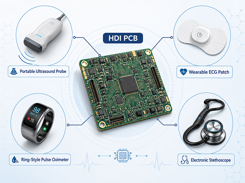
Compact wearable oximeters, especially ring-style or highly integrated designs, may also benefit from HDI. Many fingertip and handheld oximeters, however, remain compatible with standard multilayer boards.
Compact diagnostic and hearing devices may justify HDI when low-noise analog circuitry, processing, wireless connectivity, and battery management must be integrated into a tightly constrained housing.
Conditional HDI applications
Patient monitors may use HDI on compact main-processing boards with dense processors, memory, networking, display interfaces, and multiple sensor channels. Larger monitors with distributed boards often have enough routing area for conventional multilayer designs.
Infusion pumps may justify HDI in compact portable versions that combine wireless connectivity, sensing, display, and motor control. Designs with more board area and conventional packages may not need it.
Electronic stethoscopes may use HDI when the acoustic front end, DSP, wireless communication, and power management must fit inside a small chest piece. Products with separate modules or more internal space may use conventional construction.
Products that often remain compatible with conventional multilayer PCBs
Many conventional blood-pressure monitors, CPAP or BiPAP controllers, nebulizers, and TENS or EMS controllers have enough board area and moderate enough interconnect density to avoid HDI.
Compact wearable versions, highly integrated wireless variants, or designs using fine-pitch processors should still be evaluated separately. Product category alone is not a reliable HDI selection rule.
HDI is not a quality indicator for medical devices. It does not automatically improve reliability, regulatory compliance, or clinical performance. Those outcomes depend on the selected interconnect structure, materials, process controls, assembly profile, verification plan, and product-specific qualification.
What Should Be Confirmed Before Committing to HDI?
HDI decisions should be confirmed before the stack-up, component fan-out, and controlled-impedance routing are frozen. The design team and PCB fabricator should review both the electrical requirements and the proposed manufacturing process.
Design-side checks
- BGA and CSP escape routing: Confirm whether the selected ball map can be escaped with conventional through vias or whether microvia fan-out is required.
- Via-in-pad processing: Determine whether the vias must be filled, plated over, and planarized before assembly.
- Microvia geometry: Confirm finished diameter, dielectric depth, capture pad, target pad, and preferred aspect ratio with the fabricator.
- Stacked versus staggered microvias: Confirm filling, registration, and build-up requirements before fixing the structure.
- Layer stack-up: Define which layers carry high-speed signals, reference planes, power distribution, and return-current paths.
- High-speed via transitions: Compare blind vias, optimized through vias, and back drilling using the actual channel requirements.
- Assembly exposure: Consider reflow cycles, component replacement risk, and expected thermal cycling.
Fabricator capability checks
- Minimum laser-drilled via size and positional accuracy
- Preferred microvia aspect ratio
- Supported build-up and sequential lamination cycles
- Stacked and staggered microvia capability
- Via filling, plating, and planarization
- Prototype and volume-production process equivalence
- X-ray inspection for hidden structures and internal alignment
- Microsection analysis for plating and interface verification
- Electrical testing and production traceability
ISO 13485 and medical supplier qualification
For medical electronics, review whether PCB fabrication is included within the supplier’s ISO 13485 certificate scope. The certificate may not list laser drilling or sequential lamination as separate processes, so the certificate alone is not sufficient to verify HDI capability.
Supplier qualification should confirm that laser drilling, sequential lamination, via filling, inspection, process traceability, and nonconformance control are managed within the certified quality-management system.
- Check the certificate scope, validity, and certified manufacturing location.
- Confirm whether HDI steps are performed internally or subcontracted.
- Verify whether prototype and volume production use the same facility and process controls.
- Confirm what inspection and microsection records are retained for the project.
HDI adds value when routing density, package geometry, or board dimensions make conventional multilayer construction impractical. When those conditions are absent, a standard multilayer PCB usually offers a simpler, lower-risk, and more economical solution.
Start with package escape routing. If the selected BGA cannot be routed using the available through-via geometry, line width, layer count, and board area, compare an HDI build-up against alternatives such as a larger board, a different package, additional conventional layers, or back drilling where via stubs rather than routing density are the main concern.