
Medical PCB Manufacturing for Medical Devices
Home » Medical PCB Manufacturing
SugaMed manufactures rigid, HDI, flex, rigid-flex, high-Tg, and RF printed circuit boards for medical electronics. Our fabrication services support engineering prototypes, pilot builds, and repeat production, with engineering review, controlled manufacturing processes, electrical testing, and project-specific production documentation.
- 3/3 mil Trace and Space
- 0.1 mm Laser Microvias
- Controlled Impedance
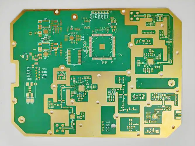
PCB Manufacturing for Medical Electronics
Medical electronics may use many of the same PCB technologies found in other advanced electronic products. The difference is often not a single material or process, but how the fabrication package, approved revisions, inspection requirements, traceability, and production records are controlled.
The appropriate PCB construction depends on the device’s electrical performance, mechanical structure, available space, thermal conditions, operating environment, and assembly process. A compact monitoring device may require HDI or rigid-flex construction, while a fixed control unit may be better served by a conventional multilayer rigid PCB.
SugaMed reviews these requirements before production so that the board construction, materials, fabrication notes, and inspection plan describe the same finished PCB.
PCB Types for Medical Devices
Different medical electronics require different board structures. We fabricate several PCB types for projects ranging from compact portable devices to larger control, sensing, communication, and power-management systems.
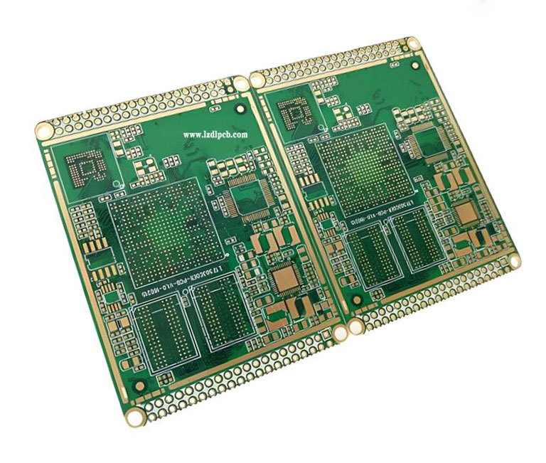
Rigid PCB
Rigid PCBs provide a stable platform for medical electronics installed in fixed enclosures, including control, sensing, communication, power-management, and user-interface circuits. Fabrication can be tailored to the required layer count, copper weight, controlled impedance, thermal conditions, and assembly process.
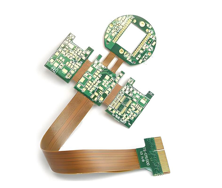
Flex and Rigid-Flex PCB
Flex and rigid-flex PCBs can connect multiple board sections, reduce separate wiring, and fit electronics into compact or three-dimensional medical device enclosures. Fabrication planning accounts for the bend location and frequency, material system, transition-zone construction, panel support, and assembly handling requirements.
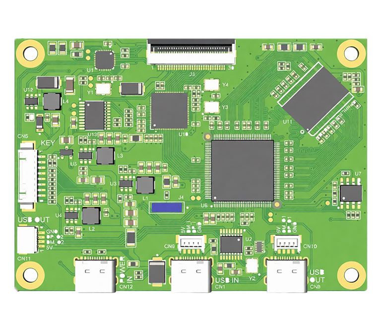
HDI PCB
HDI PCBs support compact medical electronics that require fine-pitch components, dense routing, and reduced board dimensions. During fabrication review, the microvia structure, blind and buried vias, trace and space, and build-up stack-up are evaluated against the routing density and component layout.
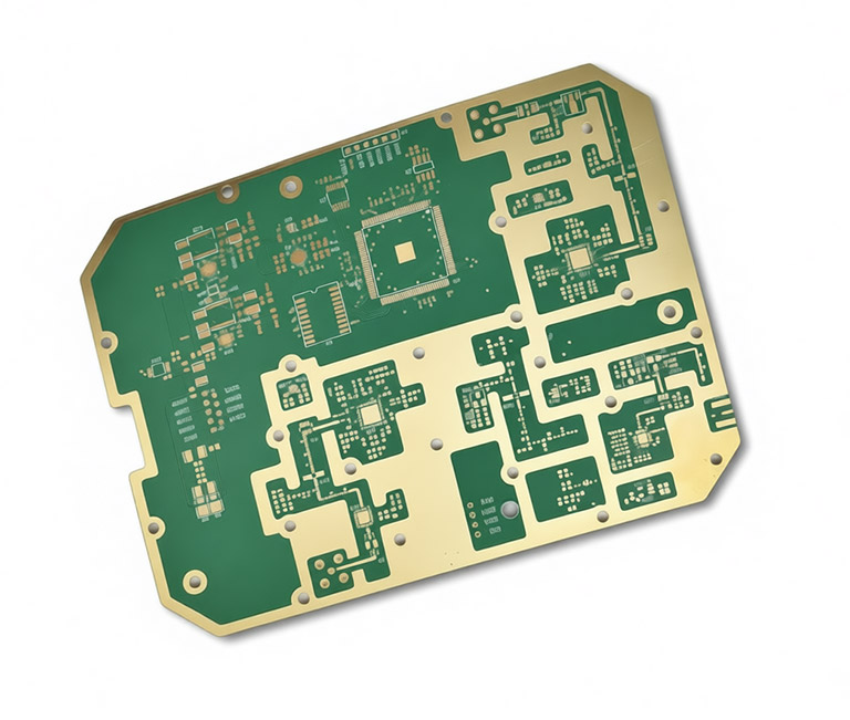
High-Frequency/RF/Microwave PCB
RF and high-frequency PCBs support wireless communication, sensing, imaging, and other circuits where signal loss and impedance stability affect performance. Before fabrication, laminate properties, stack-up, copper thickness, trace geometry, reference layers, and surface finish are reviewed together.
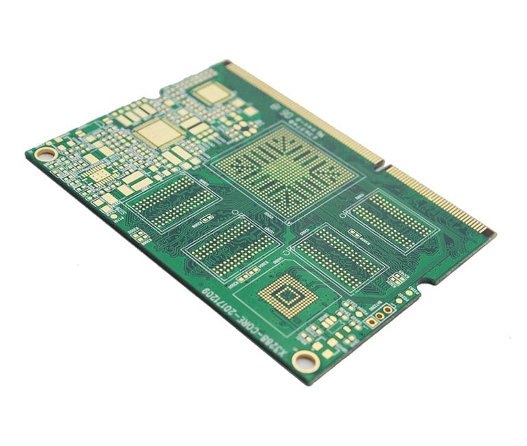
High-Tg PCB
High-Tg PCBs are used for medical electronics exposed to repeated reflow cycles, elevated operating temperatures, thermal cycling, or heat-generating components. Material and stack-up review considers Tg, decomposition temperature, thermal expansion, copper distribution, board thickness, and via structure.
Medical PCB Manufacturing Capabilities
Our fabrication capabilities cover conventional multilayer PCBs, HDI structures, blind and buried vias, controlled-impedance boards, heavy-copper constructions, and RF or low-loss materials.
The available manufacturing limits depend on the complete board construction. Material type, finished thickness, copper weight, via structure, surface finish, panel dimensions, and production quantity are reviewed together before quotation.
Board Construction
Supported PCB Layer Count
Minimum Trace and Space
Minimum Laser Microvia
Controlled-Impedance Tolerance
Supports conventional through holes, blind vias, buried vias, stacked microvias, and multilayer interconnections according to the approved stack-up.
Available HDI structures include 1+N+1, 2+N+2, 3+N+3, and any-layer designs, subject to material, via, and stack-up review. The current capability table lists up to three lamination cycles.
Materials and Surface Finishes
- Standard FR-4
- High-Tg FR-4
- Halogen-Free Laminates
- Polyimide for Flex and Rigid-Flex PCBs
- RF and Low-Loss Laminates
- ENIG
- ENEPIG
- Lead-Free HASL
- Flash Gold
- Hard Gold
- Soft Gold
- Electroplated Gold Fingers
- Immersion Silver
- Immersion Tin
- OSP
Surface-finish selection is reviewed against component pitch, storage requirements, soldering process, contact surfaces, wire-bonding needs, wear requirements, and the later PCB assembly process.
Materials and Surface Finishes
| Capability | Reference Range |
| Supported Layer Count | Up to 40 Layers |
| Finished Board Thickness | 0.4–6.0 mm |
| Copper Weight | 0.5–6 oz for standard rigid PCBs |
| Minimum Trace and Space | 3/3 mil |
| Minimum Mechanical Hole | 0.10 mm, subject to thickness and aspect ratio |
| Minimum Laser Microvia | 0.10 mm |
| Via Structures | Through, Blind, Buried, Stacked Microvias |
| Via Filling | Conductive and Non-Conductive Via Fill |
| HDI Structures | 1+N+1, 2+N+2, 3+N+3, and Any-Layer |
| Sequential Lamination | Up to 3 Lamination Cycles |
| Controlled Impedance | Standard Tolerance ±10% |
| Rigid-Flex Capability | Rigid-Flex Lamination and Flex Construction |
| RF Material Processing | Rogers, Taconic, Arlon, and Other Specified Laminates |
| Surface Finishes | ENIG, ENEPIG, OSP, Immersion Silver, Immersion Tin, Lead-Free HASL |
| Bare-Board Testing | Flying Probe or Test Fixture |
Engineering Review Before Fabrication
Before production, we review the released PCB data to confirm that the Gerber or ODB++ files, drill data, stack-up, materials, dimensions, impedance requirements, and fabrication notes describe the same board construction.
Gerber or ODB++ files, drill data, board outline, dimensions, fabrication drawings, and revision consistency are checked for missing or conflicting information.
Layer sequence, material, copper weight, finished thickness, mechanical holes, laser microvias, blind and buried vias, and aspect-ratio requirements are reviewed together.
Controlled-impedance targets, trace geometry, dielectric thickness, reference layers, coupons, and panel requirements are confirmed before the production data is released.
Medical PCB Manufacturing Process
The fundamental stages of medical PCB fabrication are similar to those used for other advanced printed circuit boards. The actual route changes with the material, layer count, via structure, surface finish, impedance requirements, and inspection plan.
Process Overview
CAM Review → Inner-Layer Imaging → Inner-Layer AOI → Lamination → Drilling → Copper Plating → Outer-Layer Imaging → Solder Mask → Surface Finish → Electrical Test → Final Inspection
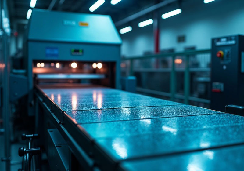
Engineering Review and Inner Layers
CAM engineers review the released fabrication data, stack-up, drill files, materials, dimensions, and panel requirements. Inner-layer circuits are then imaged and etched, followed by AOI to identify opens, shorts, and registration errors before lamination.

Lamination, Drilling, and Plating
Inner layers, cores, and prepregs are aligned and laminated under controlled temperature and pressure. Mechanical or laser drilling forms through holes, blind vias, buried vias, and microvias, followed by desmear, copper deposition, and plating.
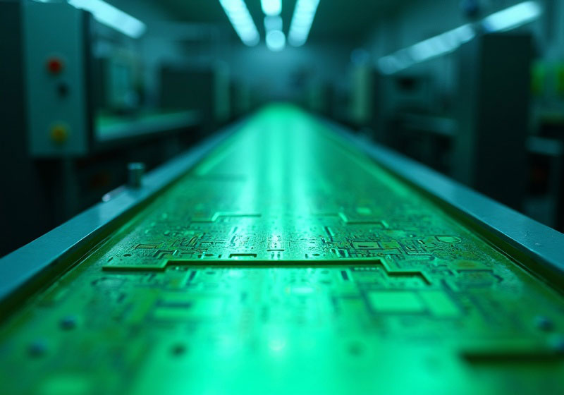
Outer Layers and Surface Finish
Outer-layer circuits are imaged, plated, etched, and inspected by AOI. Solder mask, legend, and the specified surface finish—such as ENIG, ENEPIG, immersion silver, OSP, or Lead-Free HASL—are then applied.
Electrical Testing and Final Inspection
Flying-probe or fixture testing checks electrical continuity and isolation. Dimensional inspection, solder-mask review, impedance testing, microsection analysis where required, and final visual inspection are completed before the boards are released.
PCB Manufacturing Process Quality Controls
Fabrication for medical electronics is manufactured within an ISO 13485-certified quality management system, with controls applied to materials, revisions, in-process inspection, and production records.
Manufactured within an ISO 13485-certified quality management system. Acceptance follows the project-specified IPC criteria.
Laminate, copper foil, surface-finish chemistry, and production lots can be linked to the manufacturing order according to the agreed project requirements, so material history is available for review.
Fabrication is based on the current approved Gerber or ODB++ data, drill files, stack-up, drawings, and fabrication notes. Superseded revisions are removed from the active manufacturing package.
Inspection may include inner-layer AOI, outer-layer AOI, plating checks, dimensional inspection, solder-mask inspection, electrical testing, and impedance verification where the specification requires it.
Available documentation may include material certificates, inspection records, electrical-test results, impedance reports, microsection reports, and production-lot information — provided according to the agreed project scope.
Frequently Asked Questions
What is a medical PCB?
A medical PCB is a printed circuit board used inside medical electronic devices — such as patient monitors, therapeutic equipment, and diagnostic instruments. The board itself uses conventional PCB technologies, but the fabrication package generally requires clearer control of materials, stack-up, revisions, inspection, and documentation.
What files are required for a medical PCB quotation?
A typical quotation package includes released Gerber or ODB++ files, drill data, stack-up or layer requirements, material and copper-weight information, surface finish, controlled-impedance requirements, board thickness and dimensions, quantity and target schedule, and any inspection or documentation requirements. If some files are still missing, our engineering team will identify what is required.
Does every medical PCB require IPC Class 3?
No. The IPC acceptance class should follow the project-specified requirement, which depends on the intended use and quality plan of the finished device. Some medical products are built to Class 3, others to Class 2 with additional inspection, and some use a customer-defined acceptance criteria. The class is confirmed during engineering review rather than assumed.
How do you choose between rigid, flex, rigid-flex, and HDI PCBs?
The construction is selected based on electrical performance, mechanical structure, available space, thermal environment, expected service life, and the assembly process. Rigid boards suit fixed assemblies; flex and rigid-flex fit into three-dimensional enclosures or reduce connectors; HDI is used when routing density, microvias, or fine BGA escape routing is required.
Can you manufacture prototype and low-volume medical PCBs?
Yes. Prototype and low-volume runs are supported, typically with the same fabrication data and stack-up planned for later production. Prototype builds are often used to confirm the stack-up, dimensions, surface finish, via construction, and electrical characteristics before repeat production begins.
How are controlled-impedance requirements handled?
Controlled impedance requires a defined stack-up with reference layers, controlled trace geometry, and — where required — impedance coupons and measurement reports. The impedance targets and tolerance should be listed in the fabrication drawing or a separate impedance table, so they can be reviewed together with the stack-up.
What inspection and electrical testing can be provided?
Depending on the specification, inspection may include inner-layer AOI, outer-layer AOI, plating checks, dimensional inspection, solder-mask inspection, flying-probe or bed-of-nails electrical testing, and impedance verification. The exact scope is confirmed per order rather than applied automatically to every board.
What affects medical PCB fabrication lead time?
Prototype PCB lead time depends on layer count, material, via structure, surface finish, electrical testing, and documentation requirements. A confirmed production and shipping schedule is provided after the fabrication data has been reviewed. International shipping time is quoted separately from production time.
Ready to get started on your project?
Whether you’re evaluating us for a new project or transitioning from another supplier — the starting point is a direct conversation with our engineering team.
Discuss Your Project
Share your board complexity, volumes, and regulatory requirements. We'll give you a clear picture of what we can do and what the timeline looks like.
Schedule a Facility Visit
On-site visits to our Dongguan facility can be arranged — production floor access, quality system review, and time with engineering team leads.