SMT PCB Assembly
Our engineering-driven SMT services lock in reliability at every step: we maintain ±1°C tight reflow temperature control for consistent solder joints, achieve a >98% average first-pass yield, deliver 100% full-board AOI inspection on every run, and handle 01005 micro-components with precision — all backed by full lot traceability to meet FDA 21 CFR Part 820 and ISO 13485 requirements.
- ✦ >98% First-Pass Manufacturing Yield
- ✦ ±1°C Reflow Zone Temperature Control
- ✦ 100% AOI Coverage Per Board
- ✦ 01005 Minimum Component Placement
Home » SMT Assembly
SMT Assembly Capabilities
Built for precision, scalability, and high-reliability electronics manufacturing.
Supporting 01005 components, ±0.025 mm placement accuracy, and full-process inspection (SPI, AOI, X-ray).
| Category | Parameter | Specification |
|---|---|---|
| PCB | Maximum board size | 800 × 600 × 1.6 mm, ENIG surface finish |
| Maximum layers | 40 | |
| Board types | Rigid, flex, rigid-flex | |
| Process types | SMT (single & double-sided), through-hole reflow, mixed technology, wave soldering | |
| Component | Minimum chip size | 01005 |
| Minimum QFN pitch | 0.35 mm | |
| Minimum BGA pitch | 0.35 mm | |
| Minimum connector pitch | 0.4 mm | |
| Maximum IC package | 45 × 45 mm | |
| Maximum connector length | W45 × L100 mm | |
| Package types supported | BGA, QFN, LGA, CSP, fine-pitch IC | |
| Solder Paste Printing | Print accuracy | ±18 μm |
| Minimum aperture | 01005, 0.25-pitch | |
| Solder Paste Inspection | System | Dual 3D cameras, moiré fringe projection, 2D color algorithm |
| Inspection height range | 0 – 450 μm | |
| Pick & Place | Standard accuracy | ±0.035 mm |
| IC / fine-pitch accuracy | ±0.025 mm | |
| Component size range | 01005 – W45 × L100 mm | |
| Reflow | Heating zones | 20 zones |
| Temperature control | ±1°C per zone | |
| Atmosphere | Nitrogen | |
| Thermal profile | Board-specific per substrate material and copper distribution | |
| AOI | Camera speed | 140 FPS |
| Optics | Custom telecentric lens + 5th-gen coaxial LED | |
| Coverage | 100% per board, full image archive | |
| First Article Inspection | Method | Auto-programming, automated judgment |
| Output | Auto-generated FAI report | |
| X-ray | Resolution | < 0.1 μm |
| Power | 160 kV / 10 W | |
| Mode | 2D + μCT (3D axis) | |
| Environment | ESD control | ESD-safe throughout |
| MSL handling | Per IPC/JEDEC J-STD-033, per-reel floor-life logging | |
| Volume | Range | Prototype → mass production |
Common SMT Defects — and How We Prevent Them
Real-world SMT defects can compromise product performance and long-term reliability. We identify, control, and eliminate these risks through advanced inspection, process optimization, and strict manufacturing discipline.
Paste slump → Bridging
Paste volume inconsistency collapses between pads under reflow heat, shorting adjacent signal traces. On IVD boards, a single bridge can cause measurement drift that passes functional test.
Tombstone effect → Open circuit
Asymmetric pad heating lifts one component end before the other wets, leaving a standing open joint. In portable monitors, a tombstoned bypass capacitor causes intermittent resets nearly impossible to reproduce.
Thermal non-uniformity → Cold joints
Dense copper pours on inner layers create localized heat sinks. Without adjusted profiles, those pads never fully wet — cold joints under high-pin-count BGAs often pass room-temperature test but fail at operating temperature.
Moisture absorption → Delamination
ICs stored beyond floor life absorb moisture that vaporizes during reflow, causing internal package delamination. Invisible to electrical test, but produces premature field failure under thermal cycling.
Five Stages. Three Interception Points.
End-to-End SMT Process Control with Built-in Quality Gates
Full Traceability & Production Data Recording
Every SMT production run is fully documented with detailed process data, ensuring complete traceability, audit readiness, and compliance with medical device standards.
Process Data Captured Includes:
- Solder paste lot traceability, print date, and 3D SPI inspection summary
- Reflow profile ID with full zone temperature logging
- Pick-and-place program version control and feeder change records
- AOI inspection results per board with full image archive
- X-ray inspection data for BGA and QFN packages
- MSL component handling and floor-life tracking per reel
- Equipment calibration status at time of production
What this enables
Process summary reports are generated for each order, formatted for seamless inclusion in your Device History Record (DHR).
In the event of a field issue, all process variables from the production run are fully traceable — enabling fast and accurate root cause identification.
Structured to support ISO 13485 audits and FDA inspections, with data retention aligned to your product lifecycle requirements.
Assembly Types We Support
These board types go beyond standard SMT assumptions. If yours isn’t listed, send us your files — we’ll assess it directly.
Portable patient monitors
High-density multilayer boards with 01005 passives, fine-pitch ICs, and mixed thermal mass across zones. A single reflow profile can't serve the whole board equally.
IVD instruments
Boards that undergo repeated thermal cycling in normal operation. Solder joint fatigue from CTE mismatch is the primary long-term failure mode — not initial test failure.
Thermal non-uniformity → Cold joints
Dense copper pours on inner layers create localized heat sinks. Without adjusted profiles, those pads never fully wet — cold joints under high-pin-count BGAs often pass room-temperature test but fail at operating temperature.
Moisture absorption → Delamination
ICs stored beyond floor life absorb moisture that vaporizes during reflow, causing internal package delamination. Invisible to electrical test, but produces premature field failure under thermal cycling.
Your Board Has BGA Devices?
Dense copper pours on inner layers create localized heat sinks. Without adjusted profiles, those pads never fully wet — cold joints under high-pin-count BGAs often pass room-temperature test but fail at operating temperature.
Engineering Support for Better Manufacturability
A major weakness in many SMT providers is the lack of engineering support. At Sugamed, we provide DFM (Design for Manufacturability) analysis before production.
Our Engineering Support Includes:
PCB layout review
Component footprint verification
Thermal profile optimization
Risk identification for potential defects
This proactive approach helps:
Reduce production issues
Improve yield rates
Shorten time to market
Equipment That Supports Precision — Not Just Volume
We invest in advanced SMT equipment to ensure both speed and accuracy, including:
- High-speed SMT placement machines (Yamaha / Panasonic)
- 3D SPI systems
- Advanced AOI inspection systems
- X-ray inspection systems
However, equipment alone does not guarantee quality. What matters is how these tools are integrated into a controlled and standardized manufacturing process.
FAQ
What component sizes can you handle?
Down to 01005 chips, 0.35mm pitch QFN, and 0.4mm pitch BGA. Placement accuracy is ±0.035mm (±0.025mm for ICs). Most high-density designs fall well within our capability range.
Do you support fine-pitch and high-density assemblies?
Yes. We run SPI (dual 3D camera, 0–450μm detection height) before reflow and AOI after, so any print or placement issues get caught before they become soldering problems. For dense layouts this matters a lot.
How do you control soldering quality?
Our reflow ovens have 20 heating zones with ±1°C temperature control. Profile is set per board — not a generic default. Combined with SPI and AOI inline, we catch most defects before they leave the line.
Can you handle mixed SMT and through-hole?
Yes. We support double-sided SMT, through-hole reflow, wave soldering, and combinations of the above. If your board has a mix, just share the details and we’ll confirm the process flow.
Ready to get started on your project?
Whether you’re evaluating us for a new project or transitioning from another supplier — the starting point is a direct conversation with our engineering team.
Discuss Your Project
Share your board complexity, volumes, and regulatory requirements. We'll give you a clear picture of what we can do and what the timeline looks like.
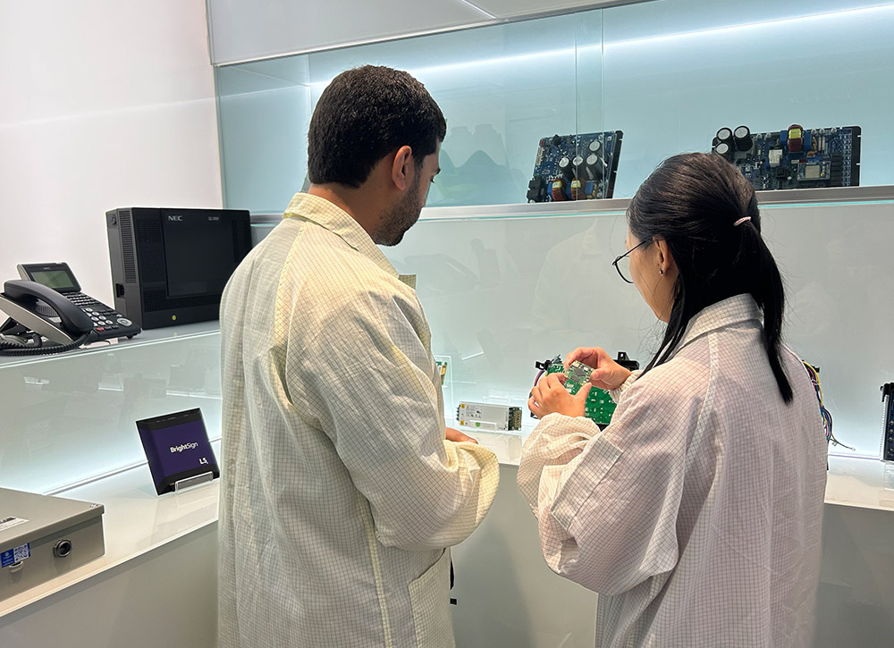
Schedule a Facility Visit
On-site visits to our Dongguan facility can be arranged — production floor access, quality system review, and time with engineering team leads.