
PCB assembly testing is not a single final inspection performed after production is complete. Different inspection and test methods target different classes of problems, from solder-paste printing and component-placement defects to electrical faults and functional failures.
For example, automated optical inspection (AOI) can identify many visible assembly defects, X-ray inspection is suited to hidden solder joints, and in-circuit test (ICT), flying probe, and functional testing each verify a different aspect of electrical condition or real-world operation.
Because no single method can detect every PCBA defect, most projects use a combination selected around the board design, component packages, production phase, volume, product requirements, and required test coverage.
Table of contents
- What Is PCBA Testing?
- Inspection, Electrical Testing, and Functional Testing
- Common PCB Assembly Test Methods at a Glance
- Major PCB Assembly Test Methods and the Problems They Detect
- How to Select a PCBA Test Strategy
- Design for Testability (DFT) and Test Coverage
- What Happens After a PCBA Fails Testing?
- PCBA Testing Considerations for Medical Electronics
- Frequently Asked Questions About PCBA Testing
- Conclusion
What Is PCBA Testing?
PCBA testing is the set of inspections and tests used during or after printed circuit board assembly to verify manufacturing quality, electrical integrity, and the board’s intended operation.
The exact sequence varies by project. A simple prototype may use visual inspection, AOI, flying probe, and an engineering-level functional check, while stable production may justify dedicated ICT fixtures and standardized functional-test equipment. These decisions are easier to manage when the manufacturer provides early PCBA engineering support.
How Does PCB Testing Differ from PCBA Testing?
The terms PCB testing and PCBA testing are sometimes used interchangeably, but they normally refer to different production stages.
Bare-board PCB testing primarily checks the fabricated circuit board itself, including continuity, insulation resistance, and conductor integrity.
PCBA testing occurs after components have been assembled. It addresses component placement, solder joints, opens and shorts, selected component values, and powered functional behavior in addition to the underlying electrical connections.
Inspection, Electrical Testing, and Functional Testing
PCB assembly quality must be verified at several levels.
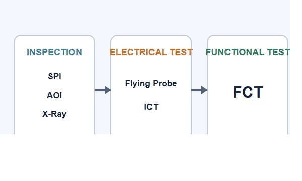
SPI, AOI, and X-ray are inspection methods used mainly to find physical defects introduced during manufacturing and assembly.
Flying probe and ICT are electrical tests used to check network connectivity, opens and shorts, and selected component characteristics.
Functional testing powers the PCBA and determines whether it operates according to defined functional requirements.
These methods complement one another. Passing AOI does not prove that the board is electrically correct, and passing ICT does not necessarily mean the complete PCBA can perform every function required by the end application.
Common PCB Assembly Test Methods at a Glance
| Method | Primary focus | Typical stage | Common use | Main limitation |
|---|---|---|---|---|
| SPI | Solder paste volume, height, and position | Before component placement | SMT printing process control | Does not inspect final solder joints |
| AOI | Component placement and visible solder defects | After placement or reflow | Most SMT assembly lines | Cannot inspect hidden joints |
| X-ray | Hidden joints and internal solder condition | After reflow | BGA, QFN, LGA, and other hidden joints | Does not prove electrical function |
| Flying Probe | Opens, shorts, and selected electrical values | Prototype or low volume | Designs that may still change | Slower than fixture-based testing |
| ICT | Electrical networks and component-level faults | Stable production | Medium- and high-volume builds | Requires test access and usually a fixture |
| FCT | Powered board operation | Final validation | Application-specific functional checks | Requires a defined test program |
| Burn-In | Early-life or time-dependent failures | Additional qualification | Selected applications | Adds time and cost |
Major PCB Assembly Test Methods and the Problems They Detect
Solder Paste Inspection (SPI)
SPI is normally performed after solder-paste printing and before component placement. It measures paste volume, height, area, and position so the manufacturing team can identify printing problems before they continue into later SMT operations.
Typical findings include insufficient paste, excessive paste, positional offset, and deposits that may lead to bridging. SPI is therefore primarily a process-control tool, not final functional testing.
Automated Optical Inspection (AOI)
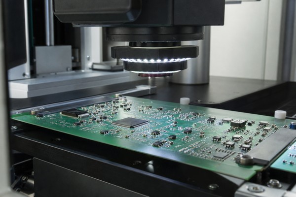
AOI on an SMT assembly line uses optical imaging to inspect assembled boards for visible manufacturing defects.
It can identify missing or shifted components, incorrect orientation or polarity, and some visible solder-joint defects. Because it is fast and provides broad visual coverage, AOI is widely used after placement and after reflow.
AOI cannot reliably inspect solder joints that are completely hidden beneath packages such as BGAs, so it does not replace X-ray inspection or later electrical and functional testing.
X-ray Inspection
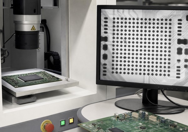
X-ray inspection can be used when solder joints or internal structures cannot be evaluated adequately by visual inspection or AOI.
It is especially useful for BGA assemblies, as well as QFN, LGA, and other packages whose joints are partially or fully hidden beneath the component. X-ray inspection can help identify bridging, insufficient solder, voiding, misalignment, and other hidden assembly abnormalities.
X-ray inspection primarily reveals assembly structure and solder-joint condition; it does not prove that electrical performance or functional behavior is correct.
Flying Probe Testing
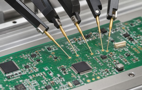
Flying probe systems use movable probes to contact test points and do not require a dedicated bed-of-nails fixture like traditional ICT.
They can check continuity, opens, shorts, and selected component values. Because a dedicated fixture is usually unnecessary, flying probe is well suited to prototype PCB assembly, engineering builds, and designs that may still change.
The trade-off is lower test speed, so fixture-based ICT is usually more efficient for high-volume, stable production.
In-Circuit Test (ICT)
ICT uses electrical test points on the PCBA to check networks and components. Depending on board design and the test program, it can find opens, shorts, incorrect component values, missing parts, and other assembly-related electrical faults.
For stable production, ICT can provide fast and repeatable testing, but it normally requires adequate test-point access and a dedicated fixture. Its economics therefore become more attractive as the PCB revision and production volume stabilize.
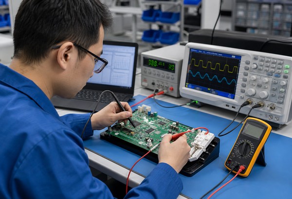
Functional Test (FCT)
Functional testing verifies the board’s actual operation while the PCBA is powered and running under defined conditions.
Depending on the product, FCT may check power rails, inputs and outputs, communication interfaces, sensors, displays, controls, actuators, firmware behavior, or other product-specific functions.
Unlike ICT, which focuses mainly on circuit and component condition, FCT asks whether the assembled board performs its intended functions.
FCT coverage is therefore highly dependent on product design, customer requirements, firmware revision, test equipment, and acceptance criteria. There is no single functional-test program that applies to every PCBA.
Additional Tests for Specific Applications
Not every project needs the same additional tests. Burn-in or aging may be used when a project needs to evaluate early-life failures or sustained operation. Boundary scan may be useful for some complex digital designs when access to physical test points is limited.
These methods are selected according to the board architecture, product requirements, coverage objectives, and production economics rather than applied automatically to every assembly.
How to Select a PCBA Test Strategy
The objective is not to use as many test methods as possible. A sound strategy combines appropriate process inspection, electrical test, and functional verification to meet defect-coverage and project requirements without unnecessary manufacturing cost or complexity.
Factors That Influence the Test Strategy
- Board complexity and component density
- Component package types, especially hidden-joint devices
- Number of test points and physical probe access
- Production volume
- Stability of the PCB revision
- Product functional complexity
- Required defect coverage
- Test-fixture cost
- Customer requirements and acceptance criteria
As a project moves from engineering builds toward stable production, the most appropriate combination of test methods may change.
Prototype and Engineering Build Stage
During prototyping, the design may change frequently, so the test approach must remain flexible. AOI can identify assembly defects, X-ray inspection may be needed for hidden joints, and flying probe is useful when a dedicated ICT fixture would be premature.
Functional checks may begin as engineering verification and later evolve into a standardized production FCT. The objective at this stage is not only a pass/fail result but also early feedback on design, assembly, and testability issues.
NPI and Low-Volume Production
As the design stabilizes, the test process becomes more standardized. Inspection criteria can be fixed, flying-probe programs refined, and engineering functional checks converted into repeatable manufacturing tests. In low-volume PCB assembly, these controls provide a practical bridge between flexible prototype testing and a repeatable production test process.
This is also the stage to assess whether production volume, available test-point access, and required test cycle time justify investing in an ICT fixture.
Test data from early production can help identify repeated process or design issues before volume increases.
Stable Production
When the PCB revision, BOM, test points, and production requirements are stable, fixture-based testing is usually more economical. A mature production flow combines process inspection, electrical test, and functional verification according to the product rather than applying every method mechanically to every board.
Design for Testability (DFT) and Test Coverage
A large part of achievable PCBA test coverage is determined before the board reaches production. Design for Testability (DFT) asks whether the PCB provides adequate access and diagnostic information for manufacturing test.
Common considerations include test points, probe pitch and accessibility, programming interfaces, connector access, diagnostic functions, safe power-up conditions, and measurable electrical or functional limits.
If test access is inadequate, coverage may be limited or require more complex fixtures and programs. DFT is therefore best addressed during PCB design and NPI rather than corrected after production has begun.
What Happens After a PCBA Fails Testing?
A failed test does not automatically identify the fault. The next step is fault isolation using inspection results, electrical measurements, component placement, solder condition, programming status, and observed functional behavior.
A typical sequence is: test failure → fault isolation → diagnosis → corrective action or rework → retest.
If routine production diagnostics cannot confirm the root cause, further failure analysis may be required. Testing establishes whether a PCBA meets defined requirements; failure analysis investigates why it did not.
PCBA Testing Considerations for Medical Electronics
The inspection and test techniques used for medical PCB assembly are fundamentally the same as those used for other electronics. SPI, AOI, X-ray, flying probe, ICT, and FCT remain standard electronics-manufacturing methods.
The difference is often in project controls: whether the test program is controlled, acceptance criteria are explicit, configuration and revisions are consistent, records are retained, and lot- or serial-level traceability is required.
Medical electronics projects may need particular control over:
- Approved test procedures and limits
- PCB and firmware revisions
- Inspection and test records
- Serial- or lot-level traceability
- Handling of nonconforming products
- Controlled changes to test programs
For PCBA manufacturing under an ISO 13485 quality management system, applicable inspection and test activities should follow controlled procedures, customer requirements, and the project’s defined quality controls.
ISO 13485 itself does not require every PCBA to undergo AOI, X-ray inspection, ICT, or FCT. The selected methods still depend on design, risk, process, and project requirements.
Frequently Asked Questions About PCBA Testing
What are the main PCBA test methods?
Common methods include SPI, AOI, X-ray inspection, flying probe, ICT, and functional testing. Selected applications may also use burn-in, aging, or boundary scan.
What is the difference between PCB inspection and PCB testing?
Inspection mainly finds physical or manufacturing defects. Electrical and functional tests verify electrical integrity and powered operation. SPI, AOI, and X-ray are primarily inspection methods; flying probe and ICT are electrical tests; FCT verifies actual function.
How should I choose between flying probe and ICT?
Flying probe is usually better for prototypes, low-volume builds, or designs that change frequently because it generally requires no dedicated fixture. ICT is better suited to stable medium- or high-volume production when fixture cost can be distributed across more units. Test access and required coverage also matter.
Can AOI replace X-ray inspection?
Not in every case. AOI is effective for visible components and solder joints, but it cannot adequately inspect joints hidden beneath packages such as BGAs. X-ray inspection is still needed when the internal condition of hidden joints must be evaluated.
When is functional testing required?
Functional testing is appropriate when the project must verify that the powered PCBA performs defined functions. Coverage depends on product functions, interfaces, firmware, test program, and customer acceptance criteria.
When should the PCBA test strategy be defined?
Ideally during PCB design and NPI. Early planning makes it easier to reserve test points, programming access, diagnostic functions, and fixture interfaces, and reduces the cost of late design changes.
Conclusion
Effective PCB assembly testing does not mean applying every available method to every board. SPI, AOI, and X-ray primarily detect manufacturing defects; flying probe and ICT identify electrical faults; and functional testing verifies that the powered PCBA operates as defined.
The final test combination should reflect board design, component packages, testability, production volume, product maturity, functional requirements, and required coverage.
The most useful question for a PCB assembly supplier and its customer is not, “Which PCBA test method is best?” It is, “Which combination of inspection and testing provides the right coverage for this product at this production stage?”