
A reliable multilayer PCB layout depends on more than fitting every connection onto the available layers. Once the layer count and stack-up have been approved, the layout still has to preserve return paths, control critical-net geometry, provide practical BGA escape routing, distribute power without bottlenecks, and stay within fabrication limits. This guide focuses on those layout-stage decisions for standard rigid multilayer PCBs. Detailed stack-up construction, prepreg selection, copper-weight planning, and impedance calculation are covered separately in the PCB Stack-up Design article.
Table of Contents
Do not continue routing against an assumed stack-up. A later change in dielectric thickness, copper thickness, or reference-plane assignment can invalidate finished routing even when the board still passes basic DRC.
- Which layers are approved for high-speed and impedance-controlled routing
- Which reference plane each controlled layer uses
- The trace widths, differential spacing, and impedance tolerances supplied or approved by the fabricator
- The permitted via structures, finished hole sizes, and drill-to-copper clearances
- Any keep-out, back-drill, via-fill, or copper-balance requirements that affect placement
Begin with a Fabricator-Approved Stack-up
Layout should begin only after the layer functions, dielectric construction, finished copper thickness, and controlled-impedance geometries have been agreed with the fabricator. The layout team does not need to repeat the full stack-up design process at this stage, but it does need a stable set of routing constraints.
For a detailed explanation of layer count, layer ordering, dielectric selection, copper weight, and controlled-impedance planning, see our PCB stack-up design guide.
Placement First, Then Routing
Component placement sets constraints that routing cannot override. Getting to routing before placement is resolved typically leads to longer critical nets, congested escape areas, additional vias, and sometimes a full layout restart.
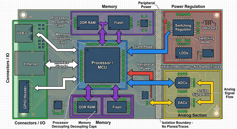
Start by positioning the parts that anchor everything else: connectors, power entry points, the main processor or controller, clock sources, high-speed peripherals, and any switching regulators. These parts define the board’s signal flow and power distribution topology. Once their locations are fixed, the routing paths for the most critical nets become visible.
Organize components by functional region. High-speed digital, analog, power, and I/O sections should not intermix freely. A switching regulator sitting in the middle of a high-speed memory area creates noise exposure that layout tweaks cannot fully mitigate after the fact.
Decoupling capacitors need to be close to the power pins they serve, but proximity alone is not sufficient. The goal is a short, low-inductance loop between the capacitor and the power and ground pins of the IC. A capacitor placed 3 mm away with a long trace winding around another component defeats its purpose regardless of how short the physical distance appears on the silkscreen.
Before routing begins, the placement should also account for:
- Sufficient escape routing channels around fine-pitch BGAs
- Via arrays for layer transitions near high-pin-count devices
- Power copper regions and their connections to the power plane
- Test point locations, especially for high-speed nets that cannot be probed after assembly
- Keep-out zones around mounting holes, edge connectors, and board cutouts
- Thermal management structures for high-dissipation components
The failure mode to avoid is treating “components fit on the board” as equivalent to “routing is feasible.” The real test is whether the critical nets can reach their destinations on appropriate layers with acceptable geometry. When that test fails mid-route, the fix usually requires moving components—which means re-running placement checks from the beginning.
Routing, Reference Planes, and Power: One Plan, Not Three
Signal routing, ground plane integrity, and power distribution interact continuously. Treating them as separate tasks leads to return path problems, power integrity failures, and EMI issues that show up late in the design cycle.
Return paths
Every high-speed or timing-sensitive signal travels as a current loop, not a single wire. The return current flows through the reference plane beneath the signal trace. If that plane is continuous and unbroken, the return current follows a tight path directly beneath the trace. If the plane has a slot, split, or cutout that the trace crosses, the return current must route around the discontinuity—which increases loop area, raises EMI risk, increases crosstalk to adjacent nets, and introduces an impedance discontinuity along the signal path.
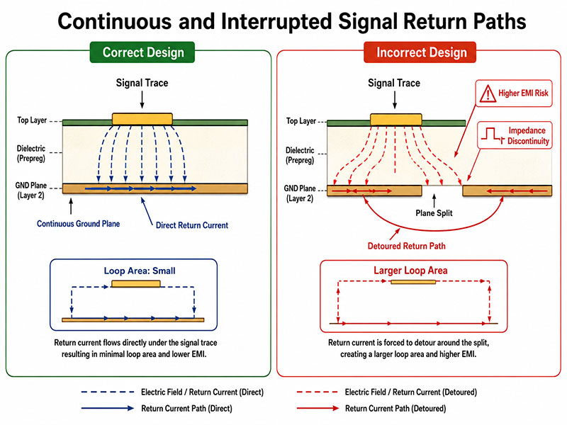
The ground plane is not a passive copper fill. Any cut made through it—for isolation, for panelization, for component clearance—should be evaluated for whether it interrupts a return current path.
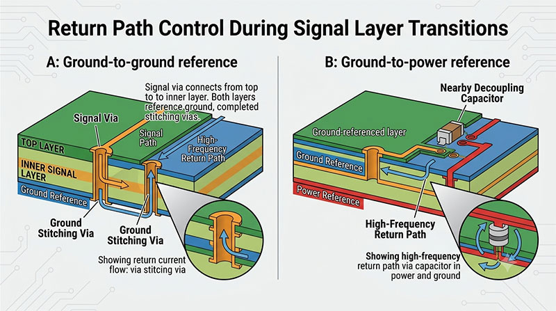
When a signal changes layers, the reference plane situation needs a specific check:
- If both the source layer and destination layer reference the same ground plane, place a ground stitching via close to the signal via. This gives the return current a direct connection between the two reference plane regions.
- If the signal moves from a layer referenced to ground to one referenced to a power plane (or the reverse), a ground stitching via alone does not solve the problem. The return current path now crosses between two different plane types. The high-frequency return must travel through decoupling capacitors that bridge the power and ground planes at that location. Make sure the necessary capacitors are placed nearby.
Routing order for critical nets
Not all nets carry equal signal integrity risk. Routing in priority order reduces the chance that a low-priority net displaces a high-priority one from its optimal layer or path.
A practical order:
- Clocks and high-speed serial interfaces (PCIe, SERDES, USB 3.x)
- Differential pairs
- Memory buses and other timing-sensitive parallel interfaces
- Analog and low-noise nets
- High-current power traces
- General-purpose signals
Route high-priority nets first, on layers where they have continuous reference planes. Lower-priority nets can use the remaining routing resources.
Trace geometry and power distribution
For controlled-impedance nets, use the approved routing geometry from the released stack-up: trace width, differential spacing, copper thickness, and reference layer. The layout task is to preserve that geometry through bends, neck-down regions, component escapes, and layer transitions—not to recalculate the stack-up during routing. See our PCB stack-up design guide for the variables that determine final trace geometry. Power-carrying traces should be sized separately according to current, copper thickness, allowable temperature rise, and the length of the current path.
Differential pair routing requires consistent geometry for the length of the pair: matched widths, matched spacing, and a consistent reference plane without transitions. Even a short section where one trace routes over a plane split or changes its spacing introduces a localized impedance discontinuity that affects signal quality at high data rates.
For parallel signal runs, the required spacing to manage crosstalk depends on the distance to the reference plane, the length of the parallel run, the signal edge rate, and the type of nets on adjacent traces. These factors interact; there is no single spacing rule that applies across all stackups and signal types. For high-speed nets with fast edge rates, model or simulate the coupling rather than relying only on geometric heuristics.
Power distribution should not depend on narrow traces. For anything beyond low-current local supply routing, use plane regions, wide copper pours, or via arrays that distribute current without creating resistive bottlenecks. Narrow necks in a power path generate localized voltage drop and heat. Power rail splits should also be reviewed for whether they create loops that couple noise into adjacent signal layers.
Choosing the Right Via Type—and What the Fabricator Can Actually Build
The via structure affects routing density, signal integrity, manufacturing complexity, and cost. The selection should be based on what the design actually requires, not on what makes routing easier in the layout tool.
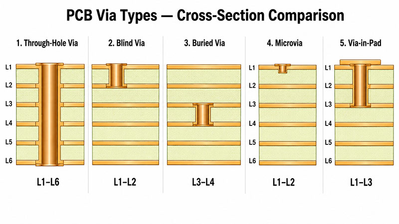
| Via type | Typical use | Main constraint |
|---|---|---|
| Through-hole | Standard multilayer routing | Barrel stub affects high-speed signals; occupies routing |
| via | space on all layers | |
| Blind via | Dense outer-to-inner escape | Higher cost; requires controlled-depth drilling |
| routing | ||
| Buried via | Internal routing channels | Requires additional lamination cycles; increases lead time |
| Microvia (HDI) | Fine-pitch BGA escape | Depth-to-diameter limits; stacking and reliability |
| constraints | ||
| Via-in-pad | Very dense component escape | Requires via fill and planarization before surface plating |
| routing |
Through-hole vias are the default for most multilayer designs. Their limitation in high-speed applications is the unused barrel section—the stub—that extends beyond the last connected layer. At high frequencies, the stub acts as a resonant element that distorts the signal. Back drilling removes the stub mechanically, but adds a process step and cost. Whether a given via requires back drilling depends on the signal frequency, the stub length relative to wavelength, and the loss budget for the net.
Blind and buried vias become relevant when through-vias cannot provide adequate routing density, particularly for BGA packages with 0.8 mm or tighter pitch. They are not a default upgrade. Before using them, confirm the finished hole diameter, the allowable aspect ratio for your board thickness, and the additional lamination requirements with the fabricator. Via-in-pad additionally requires that the via be filled and planarized before the pad is plated, which is a separate process step with its own cost and yield implications.
Microvia stacking—placing one microvia directly on top of another across multiple layers—carries reliability risks that depend on the fill material, plating quality, and thermal cycling requirements. Staggered microvias, where each via is offset from the one below, are generally more reliable but consume more lateral space. Confirm which structures the fabricator supports and under what reliability conditions before the layout is committed.
Annular ring requirements and drill-to-copper clearances vary by fabricator and board class. These are parameters to pull from the fabricator’s design rule specification, not to assume from generic guidelines.
What to Check Before the Files Leave Your Desk
A design that passes DRC in the layout tool is not necessarily ready for fabrication. The DRC catches violations against the rules you entered; it does not verify that those rules are correct, that the stackup is buildable, or that the electrical performance will meet requirements.
Electrical checks
Review controlled-impedance nets first. Verify that each net is routed on the layer and with the geometry specified in the impedance calculation, and that the impedance tolerance requirement has been discussed with the fabricator. Do not carry a default tolerance assumption into the release.
Check every high-speed net for reference plane crossings. A trace that looks clean in the routing view may cross a plane split that is not visible at the same zoom level. Review the inner layers at full board scale with reference planes visible.
For differential pairs, confirm length matching against the specified skew budget, and check that the pair maintains consistent spacing and references the same plane for its full run.
Review layer-change locations for high-speed nets. Confirm whether the reference plane changes at each via, and verify that the appropriate return path structure (stitching via or nearby decoupling) is in place.
Check power rail paths for narrow sections and isolated copper regions. A power pour that connects to the plane through a single narrow neck limits current delivery and creates a potential thermal hotspot.
DFM checks
Pull the fabricator’s current capability specification and verify against it directly:
- Minimum trace width and spacing for each copper layer
- Finished hole diameter and annular ring for all via types used
- Drill-to-copper clearance, including inner layer copper
- Copper-to-board-edge distance for all layers
- Maximum copper weight per layer relative to the dielectric thickness
Check the inner layer copper distribution. Heavily asymmetric copper distribution—where one half of an inner layer is nearly solid copper and the other half is almost empty—creates uneven resin flow during lamination and increases warping risk. Some fabricators specify a maximum copper imbalance percentage; check the requirement.
Confirm that the stackup is symmetric about the center layer. An asymmetric stackup, even with good copper balance, creates differential thermal stress during lamination. For even-layer counts this is straightforward. For designs that have ended up with an odd layer count, review this with the fabricator explicitly.
If via fill, back drilling, or controlled impedance is required, verify that each requirement appears explicitly in the fabrication notes and in the stackup documentation. Verbal alignment during DFM review does not substitute for written callouts in the release package.
Before releasing, check that the Gerber or ODB++ files, drill files, stackup drawing, and fabrication notes are mutually consistent. Layer naming, drill references, and impedance callouts should match across all documents. Inconsistencies between the drill file and the Gerber are one of the most common sources of fabrication queries.
Design release checklist
- ☐ Layer count and stackup confirmed with fabricator
- ☐ Controlled impedance tolerance agreed in writing
- ☐ No high-speed net crosses a reference plane split
- ☐ Differential pair length matching within spec
- ☐ Layer-change return paths verified for all high-speed nets
- ☐ Power rail continuity checked, no narrow necks or isolated islands
- ☐ All via types within fabricator’s confirmed capability
- ☐ Annular ring and drill-to-copper clearances verified
- ☐ Inner layer copper balance reviewed
- ☐ Fabrication notes, stackup, Gerber, and drill files consistent
FAQ
Should every signal be routed before the power planes are finalized?
No. Power distribution and signal routing should be developed together. Major power regions, regulator-to-load paths, return-current paths, and via arrays need space before general routing consumes the available channels. Final copper shapes may be refined later, but their current paths should be feasible during placement.
Can an autorouter handle a multilayer PCB layout?
An autorouter can help with lower-priority connections after placement, layer assignments, critical-net constraints, and keep-outs are established. It should not be relied on to choose reference planes, protect sensitive return paths, manage BGA escape strategy, or decide where high-speed nets should change layers.
When should blind vias or microvias be considered?
Consider them when through-hole vias prevent practical escape routing, consume too much routing area on unused layers, or create unacceptable stubs on critical channels. They should follow a confirmed fabrication need, not be introduced simply to make interactive routing easier.
What does DRC fail to verify?
DRC verifies the rules entered into the layout tool. It does not prove that the stack-up is manufacturable, that a reference plane remains continuous under a critical trace, that a power path has adequate current capacity, or that fabrication notes match the released files. Those checks require deliberate design review.
Final Design Takeaway
A sound stack-up gives the layout a workable foundation, but it does not guarantee a reliable board. Placement must preserve routing channels, high-speed traces must stay over continuous reference planes, layer transitions need a valid return path, and power copper must avoid narrow bottlenecks. Treat via selection and DFM review as layout decisions—not last-minute manufacturing corrections.
Before releasing the design, request a fabrication review covering the proposed stackup, controlled-impedance geometry, via structures, copper balance, and any special processes such as via filling or back drilling. Resolving those items before production is usually faster and less expensive than correcting them after first article.
Need a buildability check? Submit the Gerber or ODB++ files, stackup requirements, drill files, and impedance targets for a DFM review before fabrication.