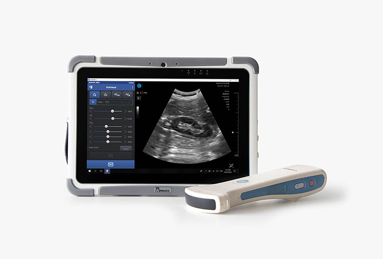
Portable Ultrasound PCB Assembly
Home » Diagnostic Devices PCBA » Portable Ultrasound PCB Assembly
PCBA manufacturing for portable ultrasound programs, from NPI prototype builds to ISO 13485 volume production.
What is Portable Ultrasound PCB Assembly?
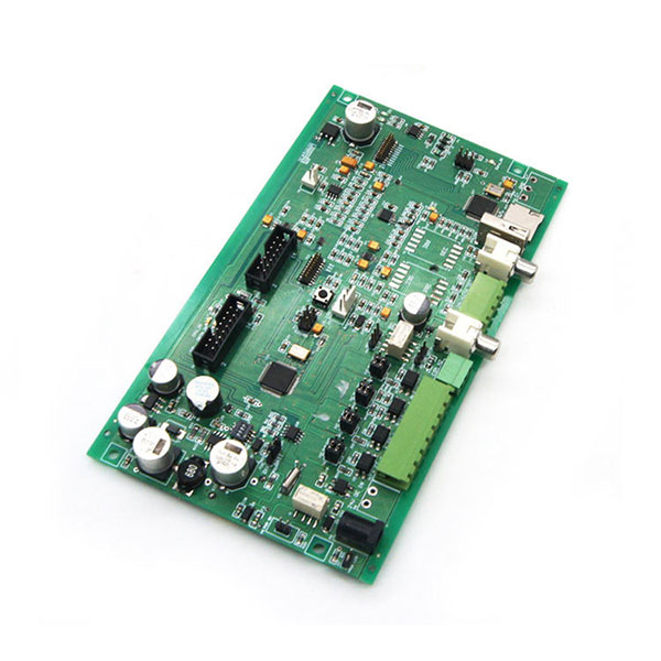
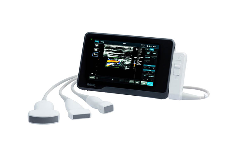
Portable ultrasound PCB assembly covers the manufacturing of the boards that form the imaging hardware in handheld, wireless, and cart-portable diagnostic devices: high-voltage transmit beamformer boards that drive piezoelectric transducer arrays with 50–100V pulses, low-noise analog receive front-end boards that amplify microvolt-range echo signals returning from tissue, digital beamforming boards built around FPGAs or custom ASICs that reconstruct the image from time-of-flight data, display and UI interface boards, wireless connectivity boards for WiFi and BLE image transmission, and battery management and power distribution boards that support extended clinical use in untethered form factors.
What distinguishes portable ultrasound board assembly from most other medical PCBA is the simultaneous presence of high-voltage transmit circuitry and a patient-contact transducer interface on the same or tightly coupled boards. The transmit stage generates switching events at amplitudes that far exceed those found in most compact medical electronics — and those events share a substrate with receive amplifiers operating at microvolt input levels. Power rail design, ground plane partitioning, transmit/receive switch placement, and HV trace routing are not layout preferences; they are manufacturing decisions that determine whether the receive path produces images or noise. These decisions are reviewed at DFM, before the layout is committed to prototype.
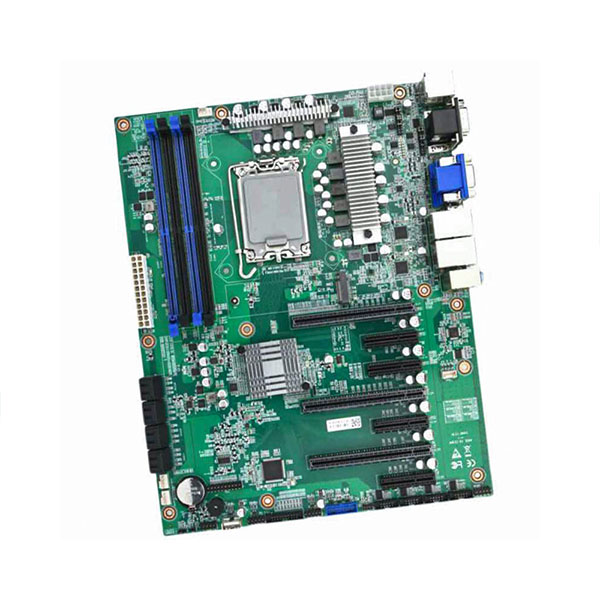
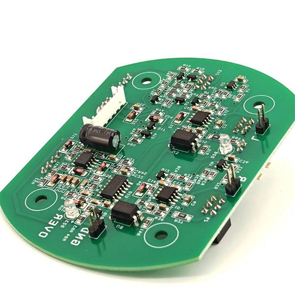
Portable Ultrasound Devices We Build PCBA For
Starting from a concept, or ready to build?
Whether you are still defining the acoustic architecture or already have production files, we can support the next step of your electronic stethoscope PCBA project.
Early-stage / NPI program
What you bring
Product concept, target acoustic specs, and form factor requirements.
What we do
Feasibility review, reference architecture discussion, prototype PCBA build, and DFM guidance.
Typical next step
Engineering discussion → prototype build → pilot run
Relevant capability
NPI support and analog front-end prototype builds where layout reflects production intent from day one.
Ready-to-build program
What you bring
Complete Gerber, BOM, and test requirements.
What we do
DFM review, medical-grade PCBA assembly, functional test, and documentation.
Typical next step
DFM review → assembly quote → production
Relevant capability
ISO 13485 assembly, IPC-A-610 Class 3, and regulatory-ready documentation.
If you’re at the concept stage with target acoustic specs but no Gerber yet — send us your specs. We review NPI programs and can discuss reference architectures before you commit to a layout.
Who builds your boards
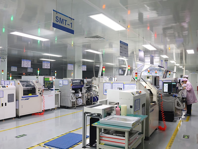
Sugamed operates a manufacturing facility with 15 Fuji and Yamaha SMT lines, 10 automatic through-hole insertion machines, multiple dedicated bonding stations, 18 PCBA assembly lines, and 40+ box-build assembly lines. Total headcount exceeds 1,100 employees.
Within this capacity, dedicated medical lines are kept separate from industrial and consumer programs — relevant for high-voltage component handling, isolation-related layout discipline, and the traceability discipline ISO 13485 requires.
We assemble PCBA across respiratory therapy, infusion, neurostimulation, patient monitoring, and emergency cardiac programs. Engineers on our medical team have worked on TENS pulse generator, EMS multi-channel output, and wearable stimulator board projects across multiple programs — including both prescription and consumer health regulatory paths.
Where Portable Ultrasound PCBA Gets Hard
High-voltage isolation failures, front-end noise, thermal limits under sustained imaging, connector wear — all identifiable earlier.
01 · HV transmit noise can reduce image clarity and affect patient safety
The transmit circuit drives ultrasound elements with 50–100V pulses. In compact handheld layouts, switching noise can couple into the receive path through power rails, ground planes, or PCB parasitic capacitance. The result may not be a failed image, but lower SNR, reduced penetration depth, and unstable image quality.
02 · Receive front-end noise can hide weak echo signals
Echo signals at the LNA input are often in the microvolt range. After 40–60 dB gain, analog noise, power ripple, ground bounce, and HV switching transients may also be amplified. The image may still look usable, but low-contrast tissue boundaries and deeper signals can become harder to detect.
03 · Sustained imaging heat can degrade performance
Handheld ultrasound boards run HV transmit, ADC, and beamforming circuits in a small enclosure with limited airflow. The real risk is not short peak heat, but sustained temperature during longer scans. Excessive heat can cause image degradation, throttling, and surface temperature concerns near patient-contact areas.
04 · Probe connector fatigue can create signal and leakage risks
The probe connector carries many mixed-voltage channels and is repeatedly plugged, unplugged, cleaned, and reused in clinical environments. Wear, poor contact resistance, solder joint fatigue, and flux residue can all cause field failures. It is also part of the patient-contact boundary, where leakage current control matters.
Compliance & Quality Standards
Medical PCBA quality is built across three layers — the standards we manufacture under, the process checkpoints embedded in every build, and the test controls applied to TENS / EMS-specific failure modes. Each layer is set at design review, not added after first article.
Layer 1 — Standards we manufacture under
- ISO 13485 — medical device QMS
- IPC-A-610 Class 3 — workmanship
- IPC-J-STD-001 — soldering compliance
- IEC 60601-1 — general safety, patient-side leakage integrated at DFM
- IEC 60601-1-2 — EMC behavior reviewed at design stage
Device-level certification sits with the customer. Manufacturing records formatted for FDA 510(k), EU MDR, and NMPA.
Layer 2 — Process checkpoints
① DFM / DFT — Analog front-end topology, MEMS acoustic interface, BLE antenna placement, RF/analog domain isolation, connector strain relief, leakage current considerations — reviewed before BOM commits.
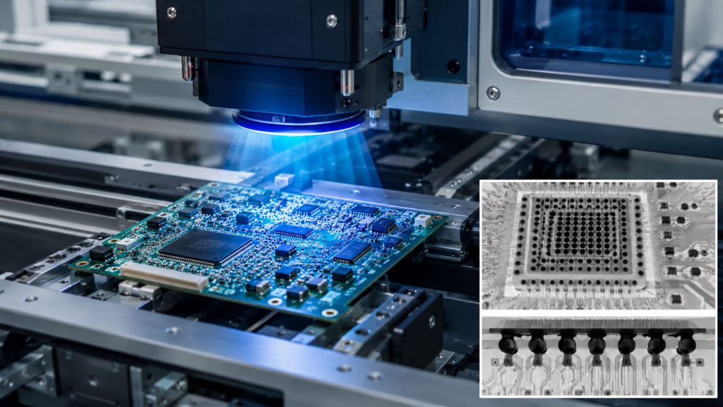
② Assembly floor — Dedicated medical lines. Inline AOI on every board. X-Ray for BGA, QFN, and high-density packages. ESD-controlled throughout. Lot-level traceability.
③ Documentation — Lot-level traceability, AOI/X-Ray archives, functional test records, process validation. Output formatted for regulatory submission workflows.
Layer 3 — Device-specific
- Functional acoustic verification — frequency response and sensitivity vs. customer spec
- Analog front-end noise floor measurement across 20–1000 Hz clinical band
- BLE coexistence test — audio verified during active BLE transmission
- Battery charging and low-battery cutoff verification
- Connector and interface inspection at first article
- Patient-side leakage current inspection where IEC 60601-1 path applies
- MEMS placement and acoustic seal verification vs. housing integration
FAQ
What's the typical lead time for a portable ultrasound prototype build?
Prototype builds typically run 3–5 weeks from Gerber receipt through functional test, depending on component availability and board complexity. Portable ultrasound programs with HV transmit stages, multi-channel ADC arrays, and FPGA-based beamforming are within standard prototype scope — lead time drivers are usually component availability for specialized analog front-end ICs or custom probe connectors.
How do you handle patient-side leakage current requirements for the probe interface?
Leakage current path analysis starts at DFM. The probe connector footprint, HV isolation geometry, and any bridging between the transmit domain and patient-contact pins are reviewed before layout is finalized. Patient-side leakage current is measured at first article on the production-representative assembly, and results are included in the build documentation package.
Do you test imaging performance, or is that the customer's responsibility?
Functional imaging verification runs against customer-defined specifications — penetration depth, frame rate, noise floor targets, and any protocol the customer defines. We build and execute the test against your targets; we do not define clinical performance thresholds. Test protocol and pass/fail criteria are agreed at DFM review, before first prototype build.
Do you support box-build and complete device assembly?
Yes. Sugamed operates 40+ box-build assembly lines. Electronic stethoscope programs requiring PCBA assembly plus final device integration — housing, acoustic path assembly, connectors, and packaging — can be handled within a single production workflow.
Start your Portable Ultrasound PCBA project
Quote from our medical PCBA engineers within 24 hours.