
In SMT assembly, solder paste must be deposited accurately on PCB pads through a stencil before components are placed. Although this step may look like a simple transfer process, the manufacturing team must control the position, area, height, volume, and repeatability of every deposit.
Insufficient paste can increase the risk of inadequate solder volume or an open-circuit defect. Excess paste can increase the risk of bridging. Even if the pick-and-place machine positions every component accurately, significant offset or inconsistency in the preceding print can still lead to soldering problems during reflow.
Solder paste printing is therefore not simply a matter of applying paste. It is a precision deposition process that requires stable control at the front end of SMT production.
Table of contents
- What Is Solder Paste Printing?
- How Does the Solder Paste Printing Process Work?
- How Is Solder Paste Printing Quality Evaluated?
- How Does Stencil Design Affect Solder Paste Deposition?
- Key Solder Paste Printing Process Parameters
- Common Solder Paste Printing Defects and Their Causes
- Why Are Fine-Pitch and High-Density PCBs Harder to Print?
- Stencil Printing vs. Solder Paste Jet Printing
- How Does SPI Control the Solder Paste Printing Process?
- How Is the Printing Process Validated During NPI?
- What Must Be Controlled in Stable Volume Production?
- Solder Paste Printing Controls for Medical Electronics
- Frequently Asked Questions About Solder Paste Printing
- What is solder paste printing in SMT?
- Which factors have the greatest influence on print quality?
- Why does insufficient solder paste occur?
- How does stencil thickness affect solder paste volume?
- What is the difference between area ratio and transfer efficiency?
- What is the difference between stencil printing and jet printing?
- Why is SPI still required after solder paste printing?
- Conclusion
What Is Solder Paste Printing?
Solder paste printing is the SMT process of transferring a controlled amount of solder paste through a stencil and onto PCB pads with a squeegee.
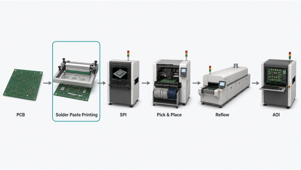
A typical SMT process can be summarized as follows:
PCB loading -> Solder paste printing -> SPI -> Component placement -> Reflow -> AOI -> Downstream inspection and testing
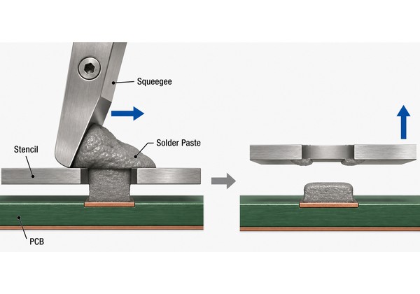
During printing, a stencil with precisely defined apertures is aligned with the PCB. A squeegee moves across the stencil and forces solder paste into the apertures. When the stencil separates from the PCB, the paste remains on the corresponding pads and provides the solder required for component placement and reflow.
A stable print does not merely mean that every pad has some paste on it. The real objective is to place the paste in the correct location and deposit an appropriate, repeatable amount on each pad.
How Does the Solder Paste Printing Process Work?
Modern SMT production normally uses an automated solder paste printer. The printing cycle includes PCB support and alignment, aperture filling, the squeegee print stroke, stencil separation, and paste release.
PCB Support and Alignment
After the PCB enters the printer, it must first be supported securely.
If the board moves, deflects, or deforms locally under squeegee pressure, the contact condition between the stencil and PCB can change and affect paste deposition. This consideration is particularly important for large or thin PCBs and double-sided PCBAs that already have components assembled on the first side.
The printer then uses fiducial marks on the PCB to align the stencil with the board so that the stencil apertures correspond as closely as possible to the pad locations.
Paste Filling and Squeegee Printing
Once alignment is complete, the squeegee moves the solder paste across the stencil surface.
During this stroke, the paste is subjected to pressure and shear from the squeegee and fills the stencil apertures. Squeegee speed, pressure, paste condition, and aperture geometry all affect the filling behavior.
There is therefore no single best squeegee speed or pressure for every PCB. These settings must be matched to the solder paste, stencil design, pad dimensions, and printing equipment.
Stencil Separation and Paste Release
After the squeegee passes, the stencil gradually separates from the PCB.
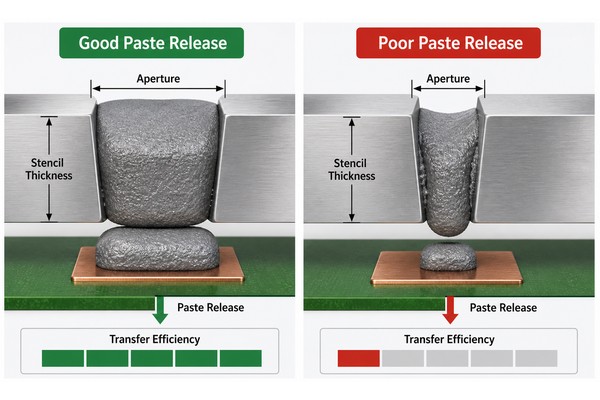
The paste inside each aperture must release cleanly onto the corresponding pad. If the paste does not separate fully from the aperture walls, the result may be an insufficient deposit, a partially missing deposit, or an abnormal deposit shape.
The complete process can be summarized as:
Support -> Alignment -> Filling -> Print stroke -> Separation -> Paste deposition
Final printing quality is the combined result of all these steps.
How Is Solder Paste Printing Quality Evaluated?
A good print must not only pass inspection once. It must remain stable and repeatable throughout continuous production.
From a manufacturing perspective, several conditions matter. Paste should be deposited accurately on the target pads, with reasonably defined edges and no obvious bridging, trailing, or contamination between adjacent pads. For pads of the same type, deposit area, height, and volume should remain consistent from board to board.
The manufacturing team must also monitor process trends rather than looking only at one PCB. If the first board prints correctly but paste volume at a specific location gradually decreases during the run, the main issue is not one isolated defective board. It is a printing process that is changing over time.
Printing quality is therefore best evaluated through a combination of:
- Actual deposit quality
- Repeatability during continuous production
- SPI measurement data
Paste area, height, volume, and positional offset do not have one universal acceptance value that applies to every PCB. The appropriate limits should be based on the PCB design, component packages, stencil design, paste type, and a validated process window.
How Does Stencil Design Affect Solder Paste Deposition?
The stencil determines where paste can pass and is one of the main factors that defines the theoretical deposit volume.
Stencil Thickness
With other conditions unchanged, a thicker stencil generally creates a larger theoretical aperture volume.
The actual volume transferred to the PCB, however, is not determined by stencil thickness alone. Aperture shape, area ratio, paste-release behavior, and transfer efficiency also matter.
For fine-pitch ICs, small passive components, and high-density pad patterns, an overly thick stencil may make paste release more difficult. Larger connectors, power components, or mechanical solder joints may require more solder.
A PCB that combines 01005 components, QFNs, BGAs, and larger devices may therefore require a compromise between significantly different paste-volume requirements.
Stencil Aperture Size and Shape
Stencil apertures are not always a simple one-to-one copy of the PCB pad dimensions.
Depending on the package and soldering requirements, some apertures may be reduced, enlarged, or modified in shape. Aperture design directly influences paste filling, release, final deposit area and volume, and the risk of bridging between adjacent pads.
Stencil design is therefore part of SMT design for manufacturability, not merely the production of a stainless-steel sheet with holes.
Area Ratio and Paste Release
As stencil apertures become smaller, the amount of paste in contact with the aperture sidewalls increases relative to the opening area.
Area ratio describes the relationship between the aperture opening area and the aperture-wall area. It is commonly used to assess how readily solder paste can release from a stencil aperture.
When aperture dimensions decrease and the area ratio becomes less favorable, more paste may remain on the aperture walls instead of transferring fully to the PCB pad. This is one reason solder paste printing for fine-pitch and very small components is more sensitive than printing on larger pads.
Area ratio should not be treated as a universal pass/fail criterion independent of materials and process conditions. Solder powder size, stencil fabrication quality, stencil surface treatment, paste properties, and printer settings can all affect actual release performance.
What Is Transfer Efficiency?
Transfer efficiency describes how much of the theoretical solder paste volume inside a stencil aperture is actually transferred to the PCB pad.
It can be expressed in simple terms as:
Actual solder paste deposit volume / Theoretical stencil aperture volume
Area ratio is mainly used to evaluate whether the aperture geometry supports good release, whereas transfer efficiency reflects the actual printing result. The deposited volume can normally be measured by 3D SPI.
During NPI or fine-pitch assembly, engineers should review not only average paste volume but also transfer efficiency and its consistency across repeated prints.
Step Stencils
When different components on the same PCB require substantially different paste volumes, a step stencil may be considered.
Small fine-pitch devices may benefit from a thinner local stencil area to improve release and bridging control, while some larger devices may require more paste. A step stencil can provide different local thicknesses on one stencil, although the decision to use one depends on the specific board design and process requirements.
Key Solder Paste Printing Process Parameters
Stencil design establishes the basic deposition conditions, but final printing performance also depends on the solder paste, PCB support, and printer settings.
Solder Paste Properties
Solder paste must exhibit two characteristics that may initially appear contradictory.
During the squeegee stroke, it must flow sufficiently to fill the stencil apertures. After it releases onto the pads, it must retain enough structural stability to resist immediate slump and spreading.
This behavior is related to viscosity, rheology, and thixotropy. Under squeegee shear, paste viscosity decreases and supports aperture filling. When the shear is removed, viscosity rises again and helps the deposit retain its shape.
Solder powder size, paste temperature, material condition, and exposure time in the production environment can also affect printing performance. Solder paste management must therefore address more than the expiration date.
PCB Support and Flatness
If the PCB is not supported securely, it may move or deflect slightly as the squeegee passes.
This can change stencil-to-PCB contact and separation behavior, affecting both deposit volume and positional consistency. Support should be confirmed during NPI, particularly for large, thin, irregularly shaped, or double-sided assemblies.
Alignment Accuracy
Stencil apertures must remain aligned with the PCB pads.
If the X/Y position or rotational alignment is incorrect, paste deposits across the entire PCB may shift away from their intended locations. Alignment error can therefore indicate the positioning condition of the complete printing system, not just one individual pad.
Squeegee Pressure and Print Speed
Squeegee pressure must be sufficient to move the paste and fill the apertures consistently without causing unnecessary stencil deflection or abnormal scraping.
Print speed affects paste shear and filling behavior. Because speed and pressure interact with stencil geometry and paste properties, they should not be set independently of the rest of the process.
Stencil Separation Speed
After printing, the way the stencil separates from the PCB affects paste release from the apertures.
If the separation conditions do not match the aperture dimensions, paste properties, and board construction, paste may remain in the stencil and produce insufficient or misshapen deposits.
Stencil Cleaning
During continuous production, paste can gradually accumulate inside the apertures or on the underside of the stencil.
If this residue is not controlled, it may contribute to blocked apertures, insufficient deposits, smearing, or an increased risk of bridging. Stencil cleaning is therefore part of continuous process control, not simply routine machine maintenance.
A fixed cleaning interval may be used as a baseline, but the interval should be validated and adjusted according to pad dimensions, aperture condition, paste behavior, and SPI trends.
Common Solder Paste Printing Defects and Their Causes
Printing defects are often influenced by more than one factor.
| Common Defect | Possible Printing-Related Causes | Potential Downstream Effect |
|---|---|---|
| Insufficient paste | Blocked aperture, incomplete release, abnormal paste condition, or unsuitable printer settings | Increased risk of insufficient solder or an open circuit |
| Excess paste | Excessive stencil thickness, unsuitable aperture design, or printing process variation | Increased bridging or short-circuit risk |
| Missing paste | Blocked aperture, incomplete filling, or release failure | Inability to form a normal solder joint |
| Print offset | Stencil-to-PCB alignment error | Deposit shifted away from the PCB pad |
| Smearing or trailing | Contamination under the stencil, inadequate PCB support, or abnormal separation | Increased risk of bridging or other reflow defects |
| Paste bridging | Excess deposit volume, insufficient spacing, or paste spreading | Increased short-circuit risk after reflow |
| Inconsistent deposits | Changes in the squeegee, solder paste, board support, or stencil cleanliness | Reduced solder-joint consistency |
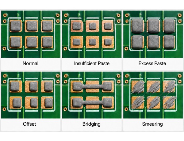
One defect does not necessarily have one unique cause. Insufficient paste, for example, may result from an aperture problem, paste condition, squeegee settings, PCB support, or separation behavior.
If SPI repeatedly reports an abnormal condition at the same location, the better response is to investigate the process cause. Simply widening the inspection limits so that the system stops reporting the condition does not resolve the underlying variation.
Why Are Fine-Pitch and High-Density PCBs Harder to Print?
As electronic products become smaller, packages such as 01005 passives, fine-pitch ICs, QFNs, and BGAs are increasingly common.
When the pads and stencil apertures become smaller, the acceptable printing window also narrows. A small positional shift or paste-volume change that has limited impact on a large pad may represent a much larger proportion of a miniature pad.
High-density SMT assembly therefore places greater emphasis on stencil aperture design, area ratio, transfer efficiency, solder powder size, PCB support, alignment, and repeatability across continuous prints.
For QFN and BGA assembly, it is also important to distinguish between inspection stages. During solder paste printing, the manufacturing team evaluates paste deposition on the package pads. After placement and reflow, inspection of hidden solder joints beneath these packages belongs to downstream methods such as X-ray.
Stencil Printing vs. Solder Paste Jet Printing
Stencil printing is the most common approach in conventional SMT production. A single stencil can deposit paste on many pads during one print cycle, making the method efficient for repeat production.
Solder paste jet printing uses program-controlled equipment to deposit paste point by point without a conventional stencil. It can provide greater flexibility for adjusting paste volume locally and may be useful for certain NPI, high-mix, or special-pad applications.
Jet-printing speed, equipment capability, paste compatibility, and production economics differ from those of stencil printing. Neither method is automatically more advanced in every situation.
For most conventional SMT volume production, stencil printing remains a mature and efficient process. Jet printing is better suited to selected manufacturing scenarios.
How Does SPI Control the Solder Paste Printing Process?
After printing, 3D solder paste inspection (SPI) measures deposit height, area, volume, and positional offset to verify the actual result.
If one region shows a continuing reduction in volume, a positional shift, or another abnormal trend, engineers can use the SPI data to investigate the stencil apertures, paste condition, PCB support, and printer settings. This creates a process-control loop:
Printing -> Measurement -> Analysis -> Adjustment
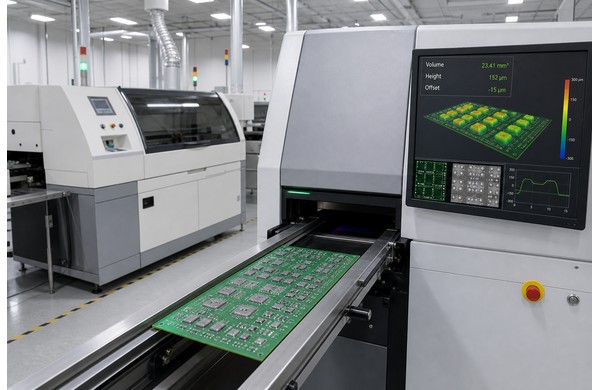
The value of SPI is not limited to rejecting one PCB with a poor print. It helps the manufacturing team detect a process that is beginning to change. For a broader view of downstream methods, see PCB assembly testing methods and their applications.
How Is the Printing Process Validated During NPI?
When a new product enters SMT production for the first time, one PCB that looks acceptable does not prove that the process is stable.
The more important question during NPI is whether the same production settings can produce repeatable results. The engineering team normally confirms stencil design, PCB support, the printer program, alignment, and SPI results on the actual product.
If selected pads repeatedly show low transfer efficiency or one area continues to show offset, the team should determine whether the cause is stencil design, paste condition, PCB support, or printer settings.
NPI is therefore not complete simply because the first article has been built. The objective is to establish a process baseline that can support stable production.
What Must Be Controlled in Stable Volume Production?
As the PCB revision, BOM, stencil, and manufacturing flow become stable, solder paste printing moves from parameter confirmation to ongoing process control.
The production team must ensure that the approved printing program is used, the stencil remains in a controlled condition, the cleaning strategy supports consistent printing, and SPI data does not show a gradual trend away from the established process window.
In mature volume production, the goal is not to change parameters frequently. It is to repeat the validated production conditions consistently and respond promptly when abnormal variation appears.
Solder Paste Printing Controls for Medical Electronics
Medical electronics use the same fundamental SMT solder paste printing technologies as other products. There is no separate category of medical-only solder paste printing.
For a medical PCB assembly with 01005 components, fine-pitch ICs, BGAs, QFNs, or a high-density layout, stencil design, paste release, and review of SPI data may require particular attention.
During NPI and volume production, the project may also require formal control of PCB and stencil revisions, printer programs, SPI programs, process records, and nonconformance handling.
Within an ISO 13485 quality management system, solder paste printing remains a standard SMT manufacturing process. The stencil, printer settings, and inspection limits should be defined according to the product design, project requirements, and validated manufacturing process. ISO 13485 does not prescribe one universal set of printing parameters.
Frequently Asked Questions About Solder Paste Printing
What is solder paste printing in SMT?
Solder paste printing is the SMT process of using a stencil and squeegee to deposit a controlled amount of paste on PCB pads. It normally takes place before component placement. After printing, SPI can verify the actual deposits before the board proceeds to pick-and-place and reflow.
Which factors have the greatest influence on print quality?
Major factors include stencil design, solder paste rheology, PCB support and alignment, squeegee pressure, print speed, stencil separation, and cleaning condition. These factors interact, so the complete process cannot be evaluated from one setting alone.
Why does insufficient solder paste occur?
Insufficient paste may be related to blocked apertures, incomplete paste release, paste condition, PCB support, or printer settings. If the same location repeatedly shows insufficient paste, the process cause should be investigated rather than treating only one PCB.
How does stencil thickness affect solder paste volume?
Stencil thickness affects the theoretical aperture volume and therefore the amount of paste that may be deposited. Actual deposit volume also depends on aperture geometry, area ratio, transfer efficiency, paste properties, and printer settings, so stencil thickness alone does not determine the final result.
What is the difference between area ratio and transfer efficiency?
Area ratio mainly helps evaluate whether an aperture geometry supports good paste release. Transfer efficiency indicates how much of the theoretical paste volume inside the aperture was actually transferred to the PCB pad. One describes a stencil-design condition; the other reflects the printing result more directly.
What is the difference between stencil printing and jet printing?
Stencil printing deposits paste on many pads in one cycle and is suitable for most SMT volume production. Jet printing deposits paste point by point under program control, does not require a conventional stencil, and offers more flexibility for local paste-volume adjustment, but its equipment and throughput characteristics are different.
Why is SPI still required after solder paste printing?
Even when printer settings have not changed, the equipment settings alone cannot confirm that the deposit on every PCB remains consistent. SPI measures deposit height, area, volume, and offset, verifies the actual result, and helps identify gradual process variation.
Conclusion
Stable solder paste printing is not determined by one best parameter.
Stencil thickness and aperture design establish the basic deposition conditions. Solder paste rheology affects filling and release. PCB support and alignment influence positional stability. Squeegee, separation, and cleaning settings affect repeatability during continuous production.
A mature SMT printing process is better understood as a continuous control loop:
Design the deposits -> Establish printing parameters -> Print -> Measure with SPI -> Analyze variation -> Adjust and stabilize the process
When evaluating a PCB assembly manufacturer’s solder paste printing capability, the printer model alone is not the most important consideration. The stronger indicator is whether the manufacturer can build a stable, repeatable process around the stencil, paste, PCB, equipment settings, and SPI data, and whether it can identify and correct process changes during production.