Prototype PCB Assembly — Built for First-Pass Success, Not Just Fast Delivery
In medical device development, a failed prototype doesn’t cost you one board. It costs you validation cycles, regulatory timelines, and months of development. We help you get it right the first time — with engineering-driven prototyping that’s production-ready from day one.
✦ Assembly in as fast as 24–72 Hours
✦ IPC-A-610 Class 3 Compliance
✦ 100% AOI + X-Ray Inspection
✦ FAI Report Included
✦ From 1 Unit
Home » Prototype PCB Assembly
Why the First PCB Prototype Decision Is the Most Critical One in Medical Development
For most PCB applications, a prototype is a low-stakes experiment — build it fast, test it, iterate. In medical device development, the stakes are fundamentally different.
The prototype stage is where your manufacturing process begins to take shape. The assembly parameters, component selections, and solder joint quality established during prototyping directly influence the data you’ll rely on when submitting your IQ/OQ/PQ process validation documentation. A prototype built with uncontrolled processes doesn’t just risk functional failure — it risks invalidating the foundation of your regulatory submission.
Consider what’s actually at risk when a medical prototype fails or requires a re-spin:
The true cost is not one board. It is your timeline.
- A single re-spin at the prototype stage typically delays the development schedule by 3 to 8 weeks when accounting for revised BOM sourcing, re-fabrication, and re-inspection.
- If the failure exposes a component selection issue — such as a footprint mismatch on a fine-pitch BGA, or an EOL (End-of-Life) part that slips into the approved component list — the impact can extend into the design verification phase, forcing additional 510(k) or CE technical file updates.
- In clinical-stage companies working against fundraising or regulatory milestones, a two-month prototype delay can have downstream consequences that go far beyond the engineering team.
Three common failure patterns we see in medical prototype projects after a failed first build with another provider:
- Late process failures: Undetected manufacturing flaws (BGA cold joints, excess voiding, inconsistent paste deposition) that only surface in late-stage testing, not basic visual checks.
- Unflagged component risks: Unreviewed BOMs lead to unplanned NRND component obsolescence, forcing costly circuit re-validation or full design re-spins months later.
- Regulatory data gaps: Missing traceability, reflow logs and SPI data leave no baseline for process validation, forcing you to restart regulatory documentation from zero.
Our Prototype PCB Assembly Capabilities
Built for high-reliability and medical-grade PCB assembly requirements
Technical capabilities
| Category | Item | Specification |
|---|---|---|
| Component & Placement | Minimum component size | 01005 (0.4 mm × 0.2 mm) |
| Fine-pitch placement |
Fine-pitch placement: down to 0.3 mm (QFP/QFN) BGA pitch: down to 0.35 mm |
|
| Supported package types | BGA, CBGA, FBGA, QFN, LGA, CSP, μBGA, Flip Chip, THT mixed assembly | |
| Placement accuracy | ±0.035 mm (standard) / ±0.025 mm (fine-pitch ICs) | |
| PCB Substrate Support | Rigid PCB | Up to 40 layers, HDI supported |
| Flex PCB | Single-sided & double-sided | |
| Rigid-flex PCB | Complex stackups for wearable & implantable designs | |
| Supported materials | FR4, Rogers, Polyimide, Ceramic | |
| Maximum board size | 800 × 600 mm | |
| Soldering Process | Reflow environment | Nitrogen reflow (O₂ < 100 ppm) |
| Reflow oven | 20-zone oven with ±1°C tight thermal control (ΔT typically within ±2–3°C across the board) | |
| Solder types | Lead-free (SAC305) & SnPb | |
| Stencil print accuracy | ±18 μm | |
| Inspection Coverage | AOI | 100% inspection for all prototype units |
| SPI | 3D paste inspection (volume, coverage, height) | |
| X-ray inspection | 2D & 3D CT for BGA & hidden joints (≤ 1 μm resolution) | |
| FAI | First Article Inspection with full report | |
| Testing Options | Flying probe test | Fixture-free, ideal for prototypes |
| Functional test (FCT) | Available upon request | |
| ICT | Supported for low-volume production transition |
Ready to scale? Explore our Low Volume PCB Assembly and Turnkey services
Production & Prototyping Capability
| Category | Item | Specification |
|---|---|---|
| Turnaround Time | Standard prototype turnaround | 5–7 business days |
| Fast-turn option | 24–72 hours (simple boards) | |
| Rapid DFM feedback | Within 12 hours after Gerber & BOM submission | |
| Production strategy |
Dedicated prototype lines to ensure fast-turn orders are not delayed by volume production |
|
| Volume Flexibility | Minimum order quantity | 1 unit |
| Typical prototype batch | 5–20 units | |
| NPI pilot runs | Up to 100 units | |
| Build flexibility | Supports multi-revision builds within a single order |
More than a PCB assembly service provider — we act as your engineering partner.
Engineering Support That Prevents Problems — Not Just Detects Them
Our pre-production engineering review is designed to surface manufacturability and compliance risks before a single component is placed — because a problem caught at DFM stage takes hours to fix; the same problem found after first article inspection takes weeks.
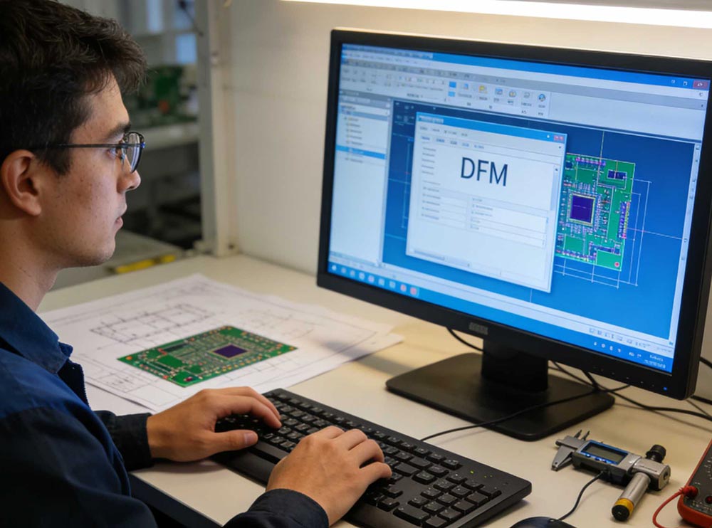
① DFM & DFA Review — Layout Risk Identification
The prototype stage is the last low-cost opportunity to correct board layout issues. A QFN thermal pad without adequate relief will produce inconsistent solder joints that no process adjustment can fix — the only solution is a board revision. Catching it before assembly costs nothing. Catching it during process validation can set your regulatory timeline back by weeks.
We review your Gerber files and BOM against assembly intent before production begins, specifically examining:
- Pad-to-ball ratio on BGA components — the primary controllable predictor of void rate
- Clearance between adjacent fine-pitch devices for rework access
- Stencil aperture geometry for paste volume optimization
- Component orientation for consistent reflow wetting behavior
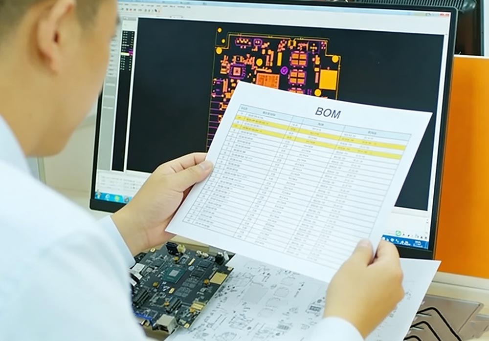
② BOM Health Check — Lifecycle & Supply Risk
The average timeline from prototype build to FDA 510(k) clearance for a Class II device is 12–18 months. A component that is fully active today may enter NRND or EOL status before your design locks for production — and if that component sits in a critical signal path, the substitution process can trigger re-characterization and additional regulatory documentation.
We run a systematic lifecycle review of every BOM line before your prototype build, and deliver:
- Lifecycle status for every active component (Active / NRND / EOL / Allocation risk)
- Recommended drop-in alternatives with matched electrical and mechanical specs
- Long-lead-time flags with pre-order recommendations for production transition
③ Component Footprint & Package Verification
Footprint mismatches are the most common cause of first-build failures in prototype assembly — and among the most damaging. A 0.1 mm discrepancy between the datasheet land pattern and the PCB pad on a 0.5 mm pitch BGA can compromise every solder joint on that package. On high-density medical boards with no rework margin, this is not a recoverable error.
We verify that every land pattern in your Gerber files matches the actual mechanical dimensions of the components in your BOM, catching:
- IPC-7351 deviations on fine-pitch components
- QFN thermal pad sizing inconsistencies that drive solder voiding
- Connector pin orientation errors that pass DRC but fail on assembly
④ Custom Reflow Profile — Per Board, Not Per Line
Medical boards increasingly combine temperature-sensitive components — MEMS sensors, RF modules, battery management ICs — with high thermal-mass connectors or ceramic capacitors on the same substrate. A generic reflow profile cannot safely serve both. Under-profiling produces cold joints; over-profiling causes delamination and component damage.
We develop a board-specific reflow profile for every prototype job, analyzing thermal mass distribution, substrate material, and component mix. The profile is validated with thermocouple data during the prototype run, then retained in our traceability system as the documented process baseline — carried forward directly into your IQ/OQ/PQ validation documentation.
Production-Level Quality Control on Every Prototype Build
Every build goes through a fixed four-stage inspection chain:
3D SPI — Paste volume, area coverage, and height deviation measured on every pad immediately after printing. Out-of-tolerance deposition triggers an automatic stop before any component is placed. Paste volume is the single largest controllable predictor of void rate — it cannot be corrected after reflow.
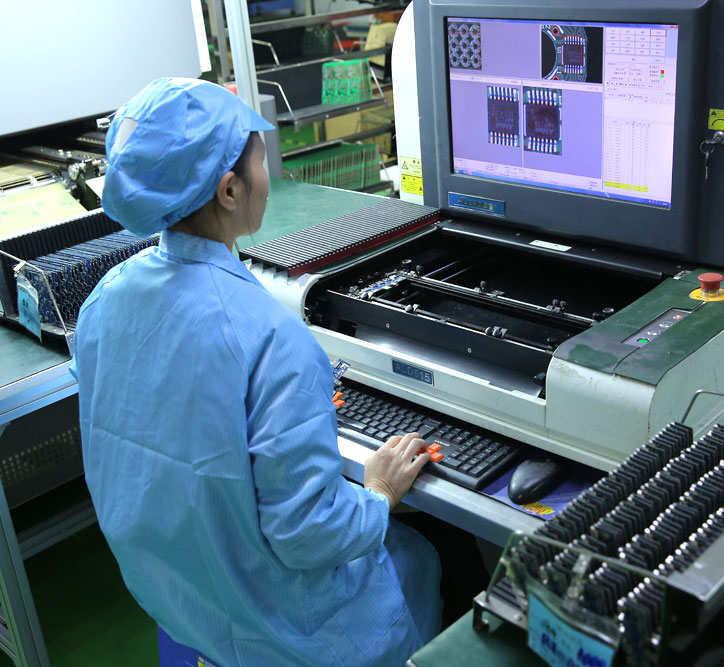
100% AOI — Every component inspected post-reflow for presence, polarity, misalignment, bridging, tombstoning, and lifted leads. 3D AOI captures co-planarity deviations that 2D systems miss.
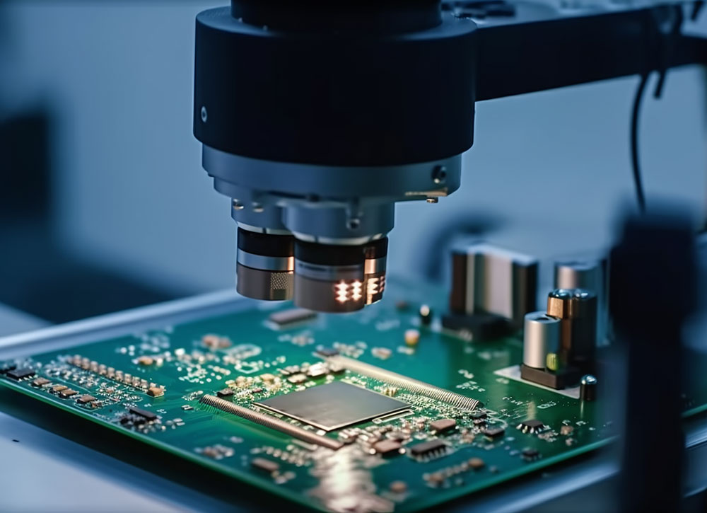
X-Ray CT Inspection — Every BGA, LGA, and QFN receives X-ray as standard, not as an add-on. 3D CT reconstruction detects internal voids, cold joints, and head-in-pillow defects. Void rate threshold: ≤ 5% per IPC-7095 Class 3.
FAI Report — Included with every build. Formatted to support submission as part of your Design History File (DHF)
Standards: IPC-A-610 Class 3 · ISO 13485:2016 · J-STD-001 · RoHS / SnPb available
Why Medical OEMs Choose Sugamed for PCB Assembly
Medical OEMs worldwide choose Sugamed because we combine high-precision process capability with the compliance infrastructure that regulatory approval demands.
Sub-micron inspection
100% X-Ray coverage with <0.1 μm resolution and μCT 3D imaging — detecting voids and cold joints invisible to conventional AOI.
Ultra-fine pitch placement
±0.025 mm IC placement accuracy. BGA down to 0.35 mm pitch, 01005 chip capability — engineered for life-critical device tolerances.
Closed-loop quality chain
SPI → AOI → FAI → X-Ray — every stage generates traceable data. Auto-generated FAI reports ready for regulatory submissions.
Production scale
21 SMT lines across China and Vietnam deliver lot-to-lot consistency from prototype validation through full-volume production.
Complex board capability
Up to 40-layer boards, 800 × 600 mm panel size, mixed-technology and Flex PCBA assembly — one partner for your most demanding designs.
Compliance-aligned QMS
Aligned with ISO 13485 and supporting customers through FDA 21 CFR Part 820 process qualification requirements.
Prototype Specifications
| Specification | Capability |
|---|---|
| Quality Standard | IPC-A-610 Class 3 — High Reliability |
| Minimum Order Quantity | 1 unit (prototype) / up to 100 units (NPI pilot) |
| Turnaround Time | As fast as 24–72 hours (fast-turn) / 5–7 business days (standard) |
| Inspection Coverage |
3D SPI + 100% AOI + X-Ray (BGA standard) + FAI Report included |
| Component Capability | 01005 / 0.35 mm BGA pitch / QFN / LGA / CSP / Rigid-Flex |
| Traceability |
Component lot tracking + process parameter records, retained 10+ years |
FAQ
Is there a minimum order?
No minimum. One board is fine. We understand prototype stages are iterative — you shouldn’t have to order 50 just to validate a design.
How fast can you turn around prototypes?
The standard lead time is approximately 7–15 days, depending on the complexity of the board.
Can you review our design before assembly?
Yes. We’ll run a DFM check and flag anything that might cause assembly issues — component orientation, pad geometry, clearance, thermal considerations. Better to catch it before parts are placed.
What if some components aren't available?
We’ll let you know as soon as we spot it during BOM review, not after you’ve been waiting a week. We can suggest alternatives, but we’ll always confirm with you before making any substitution.
Can you handle PCB fabrication and assembly together?
Yes. Keeping it under one roof speeds things up — no time lost coordinating between suppliers, and any issues that come up get resolved faster.
Ready to get started on your project?
Whether you’re evaluating us for a new project or transitioning from another supplier — the starting point is a direct conversation with our engineering team.
Discuss Your Project
Share your board complexity, volumes, and regulatory requirements. We'll give you a clear picture of what we can do and what the timeline looks like.
Schedule a Facility Visit
On-site visits to our Dongguan facility can be arranged — production floor access, quality system review, and time with engineering team leads.