
HDI boards place more interconnections into a smaller area than conventional multilayer PCBs. As dielectric layers become thinner, microvias become smaller, and line widths and spaces tighten, the margin for variation in the laminate, copper, plating, solder mask, and surface finish also becomes smaller. Understanding what each material does in the stack helps identify incompatibilities before fabrication begins.
Table of Contents
What Materials Go Into an HDI PCB
An HDI PCB normally combines six material groups: the core laminate and resin system, build-up dielectric materials, copper foil and plated copper, via-fill materials, solder mask, and the final surface finish. Conventional multilayer boards use many of the same categories, but HDI construction places tighter demands on thickness control, dimensional stability, laser-drilling behavior, plating consistency, and fine-feature imaging.
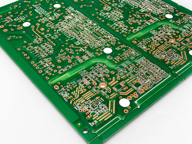
Thin build-up dielectrics are commonly used to keep laser-drilled microvias shallow and manufacturable. Depending on the stack-up and the fabricator’s qualified process, these dielectric layers may be in the tens of micrometres rather than the thicknesses used in a conventional core. Fine outer-layer conductors may also start with thinner copper so that narrow lines and spaces can be etched without excessive undercut.
The important point is that HDI is not made from one special material. It is a qualified material system. The laminate, reinforcement, build-up dielectric, copper profile, plating chemistry, via fill, solder mask, and surface finish must work together through sequential lamination, laser drilling, plating, assembly, and the product’s operating life.
Laminate, Resin, and Dielectric Build-Up Materials
Rigid HDI boards commonly start with a glass-reinforced epoxy laminate such as FR4. The resin system, glass style, resin content, and pressed dielectric thickness all influence dimensional stability, laser-drilling behaviour, moisture resistance, and dielectric consistency. FR4 is therefore not one fixed formulation. Its actual performance depends on the named material grade and supplier data. The main properties are explained in FR4 PCB material properties.
Whether an FR4 grade is suitable for HDI cannot be decided from Tg alone. The design team should also consider Td, CTE-z, T260/T288, moisture absorption, CAF resistance, resin flow, and the complete thermal history, including sequential lamination, lead-free reflow, and possible rework. High Tg material is often considered when the board will see repeated thermal exposure, fine via structures, or long service-life requirements, but it should be selected as part of the whole reliability assessment. The decision criteria are covered in the High Tg PCB material selection guide.
HDI build-up layers can use several dielectric constructions. Resin-coated copper (RCC) is one common option because its resin layer can provide a thin, controlled dielectric without woven glass directly in the laser-drilled region. Thin FR4 prepreg with copper foil, laser-processable prepreg, and other reinforced or glass-free build-up dielectrics are also used. The choice depends on the required dielectric thickness, laser-ablation behaviour, resin flow, dimensional stability, and the fabricator’s qualified lamination process.
Advanced IC package substrates may use Ajinomoto Build-up Film (ABF), but ABF should not be presented as a routine substitute for RCC or FR4 prepreg in standard PCB-level HDI fabrication. It belongs primarily to semiconductor package-substrate construction, where the feature sizes, process flow, and supplier base are different.
Polyimide becomes relevant when the product requires flex or rigid-flex construction, reduced thickness, repeated bending, or a thermal environment that justifies a different material system. It is not automatically a better choice for every rigid HDI board. The trade-offs between polyimide and FR4 are explained in when polyimide is a better choice than FR4.
Copper Foil, Plated Copper, and Via-Fill Materials
Copper selection affects both fine-line fabrication and electrical performance. Fine-feature HDI layers often begin with thinner copper, with 1/3 oz and 1/2 oz being common examples rather than universal requirements. Thinner starting copper is easier to etch into narrow lines and spaces, but the final conductor thickness also depends on subsequent pattern plating. For that reason, the fabrication drawing should distinguish between starting copper and finished copper.
Copper surface profile also matters. Standard electrodeposited copper may be suitable for many HDI designs, while reverse-treated, very-low-profile, or hyper-low-profile foil may be selected when insertion loss and impedance stability are more sensitive to conductor roughness. Rolled-annealed copper is more often associated with flex and dynamic-bending applications. Paying for lower-profile copper is most useful when the channel loss budget or flex requirement justifies it, not simply because the board is HDI.
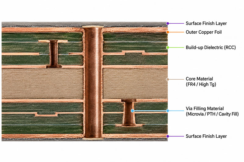
Different layers do not need to use the same copper weight. Fine-pitch signal layers may use thinner copper, while power or plane layers may require more copper to meet current and thermal requirements. The final stack-up should balance etching capability, current density, impedance, copper distribution, and lamination behaviour.
Laser-drilled microvias used in stacked or via-in-pad structures are commonly filled by copper electroplating. The filled first-tier microvia provides a flat, continuous foundation for cap plating, component pads, or a second microvia tier. Copper fill is not used only to increase current capacity; it is also important for planarisation and for the mechanical and metallurgical continuity of stacked structures.
Non-conductive epoxy fill is more commonly associated with mechanically drilled through holes, buried vias, or larger via-in-pad structures that are filled, planarised, and capped. Conductive epoxy exists for specialised applications, but it should not be presented as the default interconnect material for laser microvias. For either process, void control, plating thickness, target-pad quality, and cross-section verification become more important as the via structure becomes more complex.
Solder Mask and Surface Finish Materials
Fine-pitch HDI assembly depends not only on the metal finish but also on the solder mask. Liquid photoimageable solder mask is commonly used, and laser direct imaging may help the fabricator hold tighter registration around small pads and dense features. Important checks include the minimum solder-mask dam, pad-opening tolerance, via tenting or plugging requirements, insulation resistance, moisture resistance, and compatibility with the planned reflow profile.
The choice between solder-mask-defined and non-solder-mask-defined pads should follow the component and assembly requirements rather than a general HDI rule. On dense BGA and QFN layouts, insufficient mask registration or an unrealistically narrow mask bridge can create assembly defects even when the copper pattern itself is manufacturable.
Surface finish choice depends on what must happen at the pad after fabrication: soldering, wire bonding, repeated reflow, storage, probing, or a combination of these. ENIG is frequently used for fine-pitch HDI assemblies because it provides a flat solderable surface and works well with filled and planarised via-in-pad structures. It also requires control of the electroless nickel process to reduce black-pad risk. The detailed checks are covered in when ENIG is the right finish and what to verify before fabrication.
ENEPIG adds a palladium layer and may be selected when both soldering and wire bonding must be supported. OSP can be a cost-effective option, but its suitability depends on the specific chemistry, storage conditions, cleaning exposure, reflow atmosphere, and number of thermal cycles. Immersion silver requires control of handling, tarnish, and storage environment, while immersion tin requires control of coating quality, copper-tin intermetallic growth, and shelf life. These finishes should be evaluated individually rather than grouped as simply “lower-cost but short-life” alternatives.
IPC-6012 addresses qualification and performance requirements for finished rigid printed boards, while finish-specific requirements are covered by the applicable IPC-455x specification, customer drawing, and procurement documentation. The finish should therefore be selected and specified by its actual functional requirement, not only by the fabricator’s default recommendation.
Matching the Complete HDI Material System to the Application
Material selection should start with the product’s most demanding electrical, thermal, mechanical, and reliability condition. The aim is not to choose the “best” laminate or finish in isolation, but to create a stack that the selected fabricator can repeatedly process and verify.
For RF and high-speed modules, increasing frequency and channel length may justify a mid-loss, low-loss, or hybrid material system. The decision should be based on the channel loss budget, impedance tolerance, copper roughness, route length, and named material data. A product described as “5G” does not automatically require PTFE or a low-loss laminate on every layer.
High-density consumer and processor modules often prioritise thin build-up dielectrics, fine-line-compatible copper, low-profile foil where loss matters, and highly controlled microvia filling. Wearable or flexing products may instead require polyimide, adhesive or adhesiveless flex materials, and copper selected for bending performance.
Medical and other high-reliability projects add requirements for approved material grades, lot traceability, controlled substitutions, supplier qualification, process validation, and change control. Where the customer specification requires IPC Class 3 or an applicable medical addendum, the material system and finished-board process must support those acceptance requirements. Class 3 is not automatically required for every medical PCB.
ISO 13485 governs how the manufacturer documents, controls, and traces the selected materials and process changes; it does not prescribe a particular laminate, copper foil, via fill, solder mask, or surface finish. For a portable ultrasound, patient-monitoring, or wearable medical board, the practical question is whether the selected material system can meet the project specification consistently from prototype through volume production.
Before finalising the stack-up, confirm the laminate brand and grade, build-up dielectric, pressed thickness, starting and finished copper, copper profile, microvia fill process, solder mask capability, surface-finish specification, and any permitted substitutions. Also confirm that the prototype and production factories use the same qualified material set and process window.
Across applications, the core decisions remain the same: thermal history, signal-loss requirement, feature density, mechanical demand, traceability, and fabricator-qualified compatibility. Starting from those conditions narrows the material choices more reliably than beginning with a generic list of HDI materials.