
FR4 is a flame-retardant, woven-glass-reinforced epoxy laminate widely used as the insulating base of rigid printed circuit boards. The glass fabric provides reinforcement, while the cured resin binds the structure together and provides electrical insulation.
An FR4 PCB uses this material to support and separate its copper circuitry. FR4 is a material designation, not a specific product formulation or a four-layer board. Different FR4 grades have different thermal, electrical, and mechanical properties, so the material name alone does not define a complete PCB specification.
What FR4 Means
The letters FR refer to flame retardancy; the number identifies the material grade rather than the number of copper layers. FR4 and UL 94 V-0 are also different designations: one identifies a laminate material class, while the other describes performance in a flammability test. Check the selected material’s documented rating and applicable thickness instead of treating the FR4 label as a complete product approval.
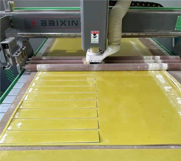
FR4 Composition and Structure
FR4 is a composite, so it has no single chemical formula or universal glass-to-resin ratio. Its main constituents are woven glass reinforcement and an epoxy-based resin system. The formulation also includes curing chemistry and may contain flame retardants, fillers, and other additives. These details vary by material grade.
In a multilayer PCB, a core is a cured laminate, often supplied with copper on both sides. Prepreg is glass fabric impregnated with partially cured resin; during lamination, the resin flows and cures to bond the layers. Glass reinforcement is therefore part of both core and prepreg, not a separate loose fabric layer in the finished board.
Copper foil forms the conductors. Solder mask covers selected outer surfaces, and a surface finish protects exposed pads. These belong to the finished PCB construction but are not the basic constituents of FR4. Glass style, resin content, and the pressed dielectric thickness all matter when defining the stack-up.
FR4 Material Properties
There is no single set of FR4 properties that applies to every board. Start with the selected laminate’s datasheet, then confirm the construction and test conditions behind the values.
| Property | What it describes | What to check |
|---|---|---|
| Tg | Glass transition of the resin system | Test method; not a continuous operating temperature |
| Td | Thermal decomposition under a defined test | Test method and weight-loss criterion |
| Dk | Relative permittivity affecting impedance and delay | Frequency, method, resin content, and construction |
| Df | Dielectric loss factor | Frequency and method; evaluate the full signal path |
| CTE | Thermal expansion in each axis | X/Y versus Z; below and above Tg |
| Thermal conductivity | Heat conduction through the material | Direction, method, and the complete heat path |
| Moisture absorption | Moisture uptake under specified conditioning | Test conditions; not a direct storage-life prediction |
Example from a Named Laminate
The following values come from Isola’s 370HR material data. They illustrate how to read a specific high-Tg FR4 datasheet; they are not universal FR4 limits or guaranteed values for every construction.
| Property | 370HR typical value | Published condition or method |
|---|---|---|
| Tg | 180 °C | DSC; IPC-TM-650 2.4.25C |
| Td | 340 °C | 5% weight loss; IPC-TM-650 2.4.24.6 |
| Dk | 4.17 | 1 GHz; IPC-TM-650 2.5.5.9 |
| Df | 0.0161 | 1 GHz; IPC-TM-650 2.5.5.9 |
| Z-axis CTE | 45 / 230 ppm/°C | Before / after Tg; IPC-TM-650 2.4.24C |
For impedance calculations, request construction-specific dielectric data and the fabricator’s proposed stack-up. A headline Dk value is not automatically the best design input. Do not directly rank materials using numbers measured at different frequencies or by different methods.
Tg and Assembly Heat Exposure
Above Tg, the resin’s stiffness and expansion behavior change. Tg is neither the temperature at which the board instantly fails nor its maximum continuous service temperature. A brief reflow excursion and years of powered operation impose different demands.
Assess Tg together with decomposition behavior, resistance to delamination, Z-axis expansion, the board structure, and the actual assembly profile. Double-sided assembly alone does not establish a universal requirement for Tg of at least 170 °C. Multiple reflow or rework cycles require a material and process combination qualified for that exposure.
FR4 Layers and Board Thickness
A two-layer or four-layer FR4 PCB has two or four copper layers, respectively. FR4 forms the insulating material between and beneath the conductors. Layer count, dielectric thickness, and finished board thickness are separate specifications. For example, a four-layer stack may contain outer signal layers and inner reference planes, separated by cured core and prepreg dielectrics.
Finished thickness should follow the enclosure, connector, stiffness, and electrical requirements. A nominal 1.6 mm board is common, but it is not mandatory or suitable for every connector. Confirm thickness and tolerance with the fabricator and check the component drawings. For layer order and dielectric construction, see our PCB stack-up design guide.
Copper weight is specified per unit area. Nominal 1 oz/ft² copper corresponds to approximately 35 µm thickness; 2 oz/ft² is approximately 70 µm. Distinguish starting foil from finished outer-layer copper, which includes plating. Current capacity depends on trace geometry, temperature rise, cooling, and surrounding copper, not on a single current threshold that dictates copper weight.
Choosing an FR4 Grade
Grade descriptions highlight different properties and can overlap. A material may be both high-Tg and halogen-free, for example. Compare the actual product specification rather than assuming one label means better performance in every respect.
- General-purpose FR4 can be a practical starting point when its thermal, electrical, and mechanical performance meets the design requirements.
- High-Tg FR4 raises the glass transition temperature, but still needs evaluation of expansion, delamination resistance, and the intended assembly process. See our high-Tg PCB fabrication page for related manufacturing considerations.
- Halogen-free materials address a specified restriction on halogen content. Confirm the applicable definition and supplier declaration separately from other compliance requirements.
- Lower-loss materials can reduce dielectric loss, but the benefit depends on the signal path and the material’s frequency-dependent data.
- High-CTI materials offer increased resistance to surface tracking under the relevant test. CTI does not by itself establish safe creepage distances for a finished product.
RoHS compliance does not automatically mean halogen-free. The European Commission’s RoHS guidance identifies specific restricted substances, including PBB and PBDE; it does not impose a blanket ban on all halogen-containing formulations. Document RoHS, REACH, and any customer halogen-free requirement separately.
Where FR4 Works Well
FR4 is widely used in control electronics, digital boards, instrumentation, and medical-device electronics. Whether it is suitable for a particular design depends on signal integrity, insulation, heat removal, assembly exposure, and service conditions. Use in a medical device does not by itself select a laminate grade or an IPC product class.
There is no universal 3 GHz or 5 GHz cutoff for FR4. A short interconnect and a long backplane trace can have very different losses at the same frequency. For digital interfaces, edge rate and the channel loss budget matter as well as data rate. Evaluate conductor loss, dielectric loss, vias, connectors, and the routing length before selecting a lower-loss substrate.
Likewise, high Tg does not make FR4 a high-conductivity heat spreader. Thermal vias, copper planes, heatsinks, and the enclosure can be important parts of an FR4 board’s heat path. Use thermal analysis to decide whether a metal-backed or ceramic substrate is justified.
FR4 Compared with Other PCB Materials
| Material option | Why consider it | Selection caution |
|---|---|---|
| FR4 glass epoxy | Broad rigid-board use and familiar processing | Check the selected grade against thermal and electrical needs |
| RF laminates | Controlled dielectric behavior or reduced RF loss | Construction and processing depend on the exact product |
| Polyimide systems | Flexible circuits or specialized heat resistance | Flexible films and reinforced rigid laminates are different constructions |
| Aluminum-backed substrates | Heat spreading from power or LED circuits | The insulating dielectric and thermal interfaces still affect heat transfer |
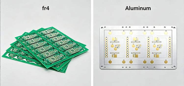
Avoid treating all Rogers products as PTFE laminates. Rogers states that RO4350B is compatible with standard epoxy/glass processing and does not require the special through-hole preparation used for PTFE materials. Material availability, stack-up, quantity, and fabrication requirements should inform a quotation; fixed cost multipliers are not reliable substitutes.
FR4 PCB Reliability Considerations
Material choice and manufacturing control work together. A higher Tg or another favorable datasheet value does not eliminate all board-level failure risks.
- Warpage can be influenced by stack-up asymmetry, copper distribution, material behavior, and processing. Review panel support and assembly conditions, and agree on acceptance criteria appropriate to the product.
- Pad cratering is cracking in the laminate beneath a copper pad. Manage board strain during handling, depaneling, testing, and assembly. Pad geometry and laminate selection need package-specific evaluation; NSMD pads are not a universal cure.
- Delamination and via damage require attention to bonding, moisture exposure, expansion, and repeated heat cycles. Agree on representative thermal and interconnect testing for the actual board construction.
- Conductive anodic filament growth can create an internal conductive path under moisture and electrical bias. Evaluate material resistance, insulation spacing, fabrication quality, and the expected environment rather than applying one universal via-pitch threshold.
For bare-board storage and moisture handling, use a procedure appropriate to the selected finish, board construction, packaging history, and supplier recommendations. IPC-1602 addresses printed-board handling and storage. Do not apply one baking temperature and duration to every FR4 PCB or substitute a component moisture-sensitivity procedure for a bare-board process. Baking, if needed, must also protect solderability.
How to Specify an FR4 PCB for Manufacturing
A useful fabrication package identifies the construction to be made and how it will be accepted. Include:
- The laminate grade, or explicit performance requirements and rules for approving equivalent materials.
- The copper layer count, stack-up, finished thickness and tolerance, and copper requirements by layer.
- Controlled-impedance targets, tolerances, and any required verification coupons or reports.
- Surface finish, solder mask, assembly heat exposure, and relevant environmental conditions.
- The applicable workmanship and acceptance requirements, including the standard revision and product class where specified.
- Required inspection records, traceability, and material or environmental compliance declarations.
If you are preparing a board for production, send the PCB files and these requirements to SugaMed for a PCB fabrication review. Confirm the proposed material and stack-up before release so that electrical design, mechanical fit, and the manufacturing specification refer to the same construction.