
Choosing between 1+N+1 and 2+N+2 comes down to one question: can a single build-up layer per side complete all the fan-out your packages require? If yes, adding a second build-up layer increases cost and manufacturing complexity without a corresponding return. If not, 2+N+2 solves a problem 1+N+1 cannot.
Table of Contents
What Is the Structural Difference Between 1+N+1 and 2+N+2?
In both structures, N refers to the central core — the inner signal and plane layers that form the base laminate. The number prefix describes how many build-up layers are added to each outer face of that core.
With 1+N+1, one build-up layer is added to each side. This creates a single microvia tier per side: laser-drilled holes connecting L1 to L2. The build-up sequence requires one lamination round after the core is complete.
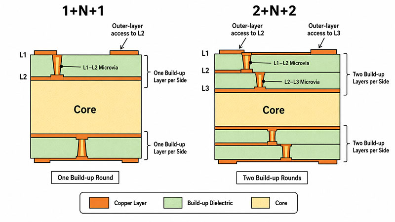
With 2+N+2, two build-up layers are added to each side. This produces two microvia tiers — L1–L2 and L2–L3. A second lamination round follows after the first build-up layer has been processed. Where a direct path from L1 to L3 is needed, the two microvias can be arranged as stacked (co-axial, one directly above the other) or staggered (offset laterally, connected by a short trace on L2).
| 1+N+1 | 2+N+2 | |
|---|---|---|
| Build-up layers per side | 1 | 2 |
| Microvia tiers per side | L1–L2 | L1–L2 and L2–L3 |
| Deepest accessible layer from outer side | L2 | L3 |
| Build-up lamination rounds | One | Two |
Fabricators count lamination cycles differently — some include the core press, others count only the build-up rounds. Confirm the definition when comparing quotes.
What Changes When a Second Build-up Layer Is Added?
Adding a second build-up layer on each side changes three things at once: routing access, manufacturing process steps, and commercial factors.
Routing access. The most direct benefit is access to a second outer routing layer. With L3 reachable from the surface, L2 can serve as a reference or power plane rather than carrying fan-out traces. In congested layouts with multiple fine-pitch packages, this separation of routing tiers can resolve channel conflicts that make a 1+N+1 layout impractical.
Manufacturing steps. Each additional build-up round adds laser drilling, copper filling, cap plating, imaging, etching, and inspection. Stacked microvia structures — where two microvias align vertically — require reliable copper fill and cap plating at the first tier before the second laser step can begin. Voids or incomplete fill at the interface create reliability risks that are difficult to detect without cross-section sampling. Acceptance criteria for these structures should be defined through the current IPC-6012 series, customer specifications, and fabrication drawings.
Commercial impact. Fabricators capable of two-round sequential build-up are fewer than those offering single-round HDI. Cost rises because of the additional process steps; lead time extends for the same reason. The actual magnitude depends on panel size, via count, fill method, and fabricator capacity. Neither figure can be estimated reliably without a direct quote.
When Is 1+N+1 Enough?
1+N+1 is sufficient when all of the following are true:
- The escape study — the process of routing each signal from a package’s ball array to an available layer — confirms that all required connections can reach routing channels through a single L1–L2 microvia transition
- L2 has enough routing capacity after reference plane requirements and via-in-pad placements are resolved (via-in-pad places the microvia directly beneath the component pad, freeing trace space on L1)
- No package on the outer layer requires access to L3 to complete its connection
These conditions are met across a broad range of designs. Industrial control boards, mid-density communication modules, and sub-systems built around packages with an open or partially depopulated ball map often qualify. A package with a relatively low ball count and adequate channel spacing may be fully escaped using 1+N+1 with via-in-pad — but package pitch alone does not determine this. The escape study does.
When 1+N+1 is viable, it is generally the better choice. The simpler process supports a broader fabricator pool, lower cost, and shorter lead times, with no functional trade-off.
What Design Conditions Justify 2+N+2?
2+N+2 is justified when the escape study shows that a second microvia tier solves a problem the first cannot.
The most common trigger: a high-density, fine-pitch package with a full ball array cannot be completely escaped using L2 alone, even after applying via-in-pad and evaluating ball-map openings. The routing channels for the remaining signals exist on L3, but a single microvia tier cannot reach them.
A second trigger occurs when L2 must serve primarily as a reference or power plane. If routing signals through L2 would break its plane continuity in a way that degrades signal integrity or PDN performance, the fan-out has nowhere to go within a 1+N+1 structure.
In designs where multiple fine-pitch devices — a processor, memory, and power management IC — compete for the same L2 routing channels, the congestion may be unresolvable without a second build-up layer.
Compact boards in medical imaging equipment and high-density processor modules are typical examples where 2+N+2 becomes the practical choice — not as a default, but because single-tier fan-out has been confirmed insufficient. Before committing, evaluate the alternatives: a larger board footprint, a different package option, or additional core signal layers. Any of these can sometimes relieve routing pressure without the cost and lead-time impact of a second build-up round.
How to Select the Right Stack-up
Work through these steps before deciding:
- Can through-via fan-out complete the layout? If yes, HDI may not be necessary at all.
- Does the escape study confirm 1+N+1 is feasible? Run the study for each fine-pitch package. Evaluate via-in-pad and available ball-map openings before concluding that a second build-up layer is needed.
- Does L2 have sufficient routing capacity? Account for reference plane and power distribution requirements before treating L2 as a pure routing resource.
- If 1+N+1 is not feasible, is 2+N+2 the most efficient solution? Compare it against a larger board, a different package, or additional core layers. The right answer is the one that solves the problem with the least additional process complexity.
- Can the target fabricator reliably produce and verify the chosen structure? Stacked microvia builds require cross-section validation. Confirm that the fabricator’s process has been qualified for your specific via diameter and capture-pad geometry.
Choose 2+N+2 because it solves a routing problem 1+N+1 cannot — not because it represents a higher tier of HDI. If the escape study confirms that single-tier build-up handles all required connections, there is no engineering basis for adding a second round.