
Choosing a surface finish shapes how well your PCB survives storage, assembly, and thermal cycling. ENIG — electroless nickel immersion gold — is one of the most common finishes for surface-mount designs, but it is not automatically the right call for every board. This article explains how ENIG is built, when it is worth specifying, what can go wrong, and how it compares with alternatives so you can make the decision before fabrication begins.
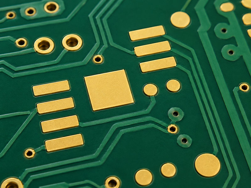
Table of Contents
What Is an ENIG PCB Finish?
ENIG stands for electroless nickel immersion gold. It replaces exposed copper on PCB pads with two deposited layers: nickel first, then a thin layer of gold on top.
The two layers serve different functions:
| Layer | Function |
|---|---|
| Electroless nickel | Diffusion barrier; solderable base layer |
| Immersion gold | Protects the nickel surface from oxidation before assembly |
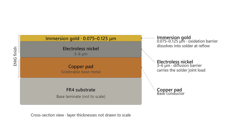
The gold layer is thin — IPC-4552A specifies a minimum of 0.05 µm, with a typical production range of 0.075–0.125 µm. Gold above 0.125 µm is not recommended: at that thickness the immersion process becomes more aggressive and increases the risk of nickel corrosion. Gold’s job is to keep the nickel surface clean and wettable until the board reaches assembly. When solder is reflowed, it bonds to the nickel. The gold dissolves into the joint during reflow.
The nickel layer carries the actual soldering load. IPC-4552A sets a minimum nickel thickness of 3.0 µm, with typical production targets ranging from 3 to 6 µm.
ENIG is sometimes confused with hard gold. Hard gold uses an electrolytic process to deposit a much thicker layer — typically 0.75–1.27 µm (30–50 µin) — for wear resistance. It is designed for edge connectors and repeated contact areas, not solder joints. The two finishes are not interchangeable.
How the ENIG Finish Is Applied
ENIG is deposited through a sequential chemical process, not conventional electroplating. The process does not require electrical current through the board, which is why it produces uniform coverage across all exposed pad geometries — including small BGA pads and fine-pitch SMT lands where plating uniformity matters most.
The key steps:
- Copper surface cleaning
- Micro-etching to improve adhesion
- Catalyst activation
- Electroless nickel deposition via autocatalytic chemical reaction
- Immersion gold deposition via chemical exchange — gold ions displace surface nickel atoms
- Washing, drying, and final inspection
Bath chemistry, temperature, immersion time, and contamination levels all affect the final deposit. Nickel thickness, gold coverage, and defect risk are outputs of process control. This is where black pad originates — covered in the next section.
For buyers, this process dependency matters at the sourcing stage. A supplier who monitors bath chemistry, tracks phosphorus content in the nickel deposit, and controls plating cycle times will produce more consistent results than one who does not. The same “ENIG” callout on two different suppliers’ fab drawings can produce very different results.
When ENIG Is the Right Finish — and When It Is Not
ENIG is worth specifying when pad flatness, storage life, and assembly reliability all matter at once. It is not the only finish that delivers any single one of those properties.
Where ENIG performs well:
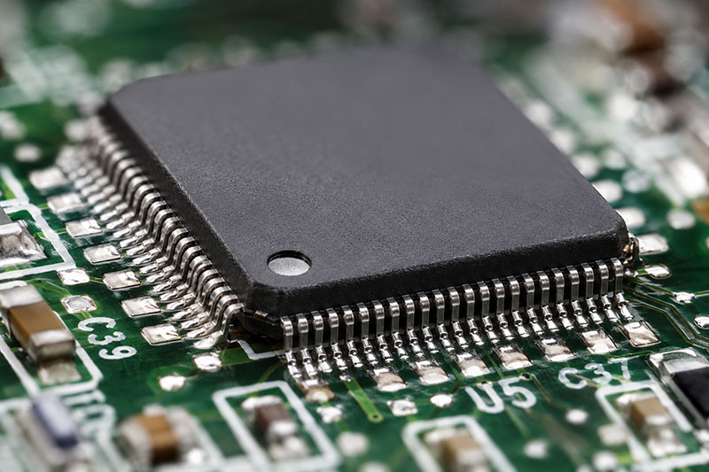
- BGA and QFN packages, where pad flatness directly affects solder joint uniformity
- Fine-pitch SMT — 0.4 mm pitch QFN, 0.5 mm pitch BGA — where an uneven surface causes bridging
- HDI PCBs with dense via-in-pad designs
- Boards stored for weeks or months before assembly
- Lead-free reflow profiles at 245–260°C
- Applications where multiple reflow or rework cycles are expected
- Higher-reliability categories: medical electronics, industrial controls, automotive, and communication hardware
Where ENIG adds cost without proportional benefit:
| Choose ENIG When | ENIG May Not Be Necessary When |
|---|---|
| BGA, QFN, or fine-pitch components are present | The board uses coarse-pitch or through-hole components only |
| Pad flatness directly affects assembly yield | Unit cost is the primary constraint |
| Extended storage before assembly is expected | Boards ship directly to assembly within a short window |
| Multiple reflow or rework cycles are required | Standard HASL reliability meets the product requirement |
| HDI or high-density SMT layout | Simple, single-sided or low-complexity design |
HASL (hot air solder leveling) costs less and works reliably for many standard designs. OSP (organic solderability preservative) is flat, inexpensive, and compatible with lead-free assembly — it fits high-volume boards assembled quickly after fabrication. The cost premium for ENIG is roughly 15–30% over HASL, depending on board size and panel utilization. On a high-volume run, that difference compounds quickly.
ENIG Risks and Quality Requirements
ENIG’s main failure mode is black pad — and it is more common than many buyers expect.
What black pad is: Abnormal corrosion of the nickel layer during or after the immersion gold step. The corrosion creates a brittle nickel surface beneath the gold. Solder joints formed on this surface may look acceptable after reflow and pass initial electrical test, then fracture at the pad-solder interface during vibration testing, thermal cycling, or field use.
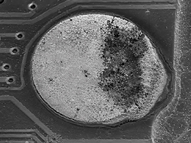
Black pad is a latent failure. The defect is not always visible. It does not always show up in standard post-reflow inspection.
The root cause is typically high phosphorus content in the electroless nickel deposit combined with aggressive gold bath chemistry. IPC-4552 recommends a phosphorus content of 7–9% by weight; content above approximately 10% correlates with higher corrosion risk. Suppliers who monitor bath chemistry, control rinse steps, and track plating cycle parameters reduce this risk — but no supplier eliminates it entirely.
Key quality parameters to verify before ordering:
| Parameter | What to Confirm |
|---|---|
| Nickel thickness | 3–6 µm; verify with XRF or microsection |
| Gold thickness | 0.075–0.125 µm typical; minimum 0.05 µm per IPC-4552A; do not exceed 0.125 µm |
| Surface condition | No discoloration, exposed nickel, or contamination |
| Process standard | IPC-4552A compliance |
| Solderability testing | Per IPC J-STD-003 if the application requires it |
| Batch traceability | Plating date, bath number, and inspection records |
Questions to ask your PCB supplier before placing the order:
- What nickel and gold thickness ranges do you target and control in production?
- Do you manufacture ENIG to IPC-4552A?
- Do you verify coating thickness by XRF on every panel or by sampling?
- How do you monitor nickel phosphorus content?
- Can you provide plating records and inspection reports with the order?
A supplier who cannot state their controlled thickness range or measurement method is worth scrutinizing before committing to a reliability-sensitive design. ENIG requirements belong in the purchase order as a documented specification, not just a fab note on the Gerber files.
ENIG vs Other PCB Surface Finishes
Surface finish selection involves trade-offs between cost, shelf life, pad flatness, and process compatibility. ENIG performs well in three of those four — cost is where it falls behind.
| Finish | Strengths | Limitations | Best Fit |
|---|---|---|---|
| ENIG | Flat surface, good solderability, long shelf life | Higher cost; black pad risk if process is poorly controlled | BGA, fine-pitch, HDI, reliability-sensitive boards |
| HASL (lead-free) | Low cost, widely available, robust solderability | Uneven surface, less suitable for fine-pitch pads | Standard through-hole and coarse-pitch SMT |
| OSP | Very flat, low cost, environmentally clean | Short shelf life, degrades with repeated heat cycles, handling-sensitive | High-volume SMT assembled quickly after fabrication |
| Immersion silver | Flat, good electrical and RF performance | Tarnish risk, sensitive to handling and contamination | High-speed, RF, and fine-pitch designs |
| ENEPIG | Supports soldering and gold wire bonding, lower black pad risk | Higher cost and more process steps than ENIG | Wire bonding, high-reliability assemblies |
| Hard gold | High wear resistance | Not intended for solder joints; expensive | Edge connectors, gold fingers, mechanical contacts |
A few distinctions that often get overlooked:
ENIG vs immersion silver: Both provide flat surfaces and support fine-pitch assembly. Immersion silver costs less, but tarnishes under atmospheric exposure and is more sensitive to handling contamination. When storage time between fabrication and assembly is uncertain, ENIG is more forgiving.
ENIG vs ENEPIG: ENEPIG adds a palladium layer between nickel and gold. This reduces corrosion at the nickel surface — addressing the black pad mechanism directly — and makes the finish suitable for gold wire bonding. For wire-bonding applications, ENEPIG is the standard choice. Standard ENIG is not recommended for gold wire bonding because the thin gold layer and underlying nickel surface are not optimized for bonding reliability.
ENIG vs OSP: OSP works well when boards move quickly from fabrication to assembly in a controlled process. A second or third reflow cycle degrades the OSP coating, which increases solderability risk for boards that require rework. ENIG handles multiple thermal cycles with less degradation.
What to Specify When Ordering ENIG PCBs
Writing “ENIG” on the fab drawing is the starting point, not the complete specification. Missing detail gets filled in by supplier interpretation — and supplier interpretation produces variation.
Specification checklist for RFQ and fabrication notes:
- Surface finish: ENIG per IPC-4552A (or applicable customer standard)
- Nickel thickness range (typically 3–6 µm; confirm supplier’s controlled target)
- Gold thickness range (typical production target 0.075–0.125 µm; minimum 0.05 µm per IPC-4552A)
- Identify BGA, QFN, and fine-pitch pad areas explicitly in the fab drawing or assembly notes
- State lead-free assembly requirement if applicable
- State expected storage duration before assembly
- Request XRF verification report when dimensional control is critical
- Specify whether plating batch records and inspection documentation are required with delivery
- Confirm whether any board areas require a selective finish — hard gold on edge fingers requires a separate callout
Board-type considerations worth confirming with your supplier:
For HDI PCBs with via-in-pad, confirm that ENIG can be applied uniformly over filled and planarized vias. For rigid-flex boards, verify process compatibility with the polyimide base material. For high-frequency boards on Rogers or PTFE laminates, confirm that the chemical process does not affect the base laminate — some laminates have chemical resistance limits that restrict the plating chemistry options. For high-Tg FR4, the ENIG process is generally compatible, but confirm when the laminate supplier specifies chemical resistance limits.
Conclusion
ENIG delivers a flat, oxidation-resistant, solderable surface that holds up through lead-free reflow and extended storage — which is why it is the default finish for BGA, QFN, and fine-pitch SMT on boards where assembly yield and shelf life matter. It is not the right answer for simple, cost-sensitive designs where HASL or OSP will do the same job for less.
The result depends less on calling out ENIG in your fab notes and more on whether your supplier controls nickel and gold thickness, monitors plating chemistry, and documents the process. Specify ENIG with IPC-4552A as the referenced standard, confirm thickness ranges and verification methods, and request XRF records before your first production run.
FAQ
Is ENIG better than HASL?
For BGA, QFN, and fine-pitch components, yes. ENIG’s flat surface reduces assembly defects that HASL’s uneven coating can cause. For simpler boards with coarse-pitch or through-hole components, HASL is sufficient and costs less.
What causes black pad in ENIG?
Black pad results from abnormal corrosion of the nickel layer during or after immersion gold deposition. High phosphorus content in the nickel deposit and aggressive gold bath chemistry are the primary contributors. The failure does not always appear visually before assembly — it shows up as brittle solder joints under mechanical stress.
Is ENIG the same as hard gold?
No. ENIG uses a thin immersion gold layer (0.075–0.125 µm typical) over electroless nickel and is designed for soldering. Hard gold uses an electrolytic process to deposit a thicker layer (typically 0.75–1.27 µm) for wear resistance — it is intended for edge connectors and contact areas, not solder joints.
What thickness should ENIG be?
IPC-4552A specifies a minimum nickel thickness of 3.0 µm (typical production range 3–6 µm) and a minimum gold thickness of 0.05 µm, with a typical production target of 0.075–0.125 µm. Gold above 0.125 µm increases nickel corrosion risk and is not recommended. Confirm the supplier’s controlled production range and request XRF verification.
Can ENIG be used for BGA and fine-pitch components?
Yes. Pad flatness is one of the main reasons ENIG is selected for BGA, 0.4 mm pitch QFN, and other fine-pitch packages where surface variation affects solder joint uniformity.
Can ENIG be used for gold wire bonding?
Standard ENIG is not recommended for gold wire bonding. ENEPIG is the standard choice when reliable gold wire bonding is required.