
How does a bare PCB become a fully assembled PCBA populated with electronic components? For most modern electronic products, the process relies on SMT.
SMT, or Surface Mount Technology, is one of the most widely used PCB assembly methods in electronics manufacturing today. Unlike traditional through-hole technology, SMD components are mounted directly onto pads on the surface of the PCB and then soldered using processes such as reflow soldering.
However, SMT is more than simply “placing components.” The complete process includes a series of connected steps, from solder paste printing and component placement to reflow soldering, AOI, X-ray inspection, and electrical testing.
A typical SMT process can be summarized as follows:
PCB loading → Solder paste printing → SPI → SMT placement → Reflow soldering → AOI → X-ray inspection (if required) → Testing → Final inspection
Not every PCB follows exactly the same route. The final process depends on whether the board uses single-sided or double-sided SMT, whether it includes THT components, the component package types, and the required testing procedures.
What Is an SMT Production Line?
An SMT production line is an integrated manufacturing system made up of equipment such as solder paste printers, pick-and-place machines, reflow ovens, inspection systems, testing equipment, and PCB loading and unloading machines.
In the early days of SMT, inspection capabilities were relatively limited. As smaller components such as 0201 and 01005 packages, along with bottom-terminated packages such as BGA, QFN, and LGA, have become more common, SPI, 3D AOI, and X-ray inspection have become important parts of many production lines.
Highly automated lines can also connect equipment through conveyor systems and integrate barcodes, serial numbers, or MES software to track materials, production batches, and test results.
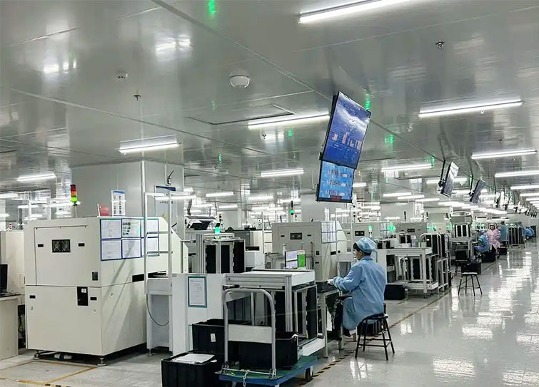
The following sections describe the typical SMT assembly sequence and explain the equipment used at each stage.
Basic SMT Assembly Process
1. PCB Loading
SMT production begins by feeding the PCB into the production line.
For mass production, an automatic PCB loader is commonly used. PCBs are placed in a magazine, and the loader feeds them one by one into the next process at a controlled rate. This reduces manual handling and helps maintain a consistent production rhythm.
For prototypes and small production runs, PCBs may also be loaded manually.
2. Solder Paste Printing
Solder paste printing is usually the first major process in SMT assembly.
The primary equipment used is a solder paste printer. It uses a stencil to transfer a controlled amount of solder paste through openings onto the corresponding PCB pads. This prepares the board for component placement and reflow soldering.
Solder paste is mainly made up of solder alloy powder, flux, and other additives. During reflow soldering, the solder melts and forms the final solder joints.
Although solder paste printing may appear straightforward, it has a direct impact on soldering quality. Too little solder can cause insufficient solder or open circuits, while too much solder increases the risk of bridging. Misalignment can also affect fine-pitch and miniature components.
For fine-pitch ICs, small components, and high-density PCBs, stencil thickness, aperture design, and printing parameters must be carefully controlled.
3. SPI Solder Paste Inspection
After printing, the solder paste deposit can be checked using SPI (Solder Paste Inspection) equipment.
Typical inspection items include solder paste height, area, volume, positional offset, and print completeness.
Many soldering defects found after reflow actually originate during the solder paste printing stage.
Detecting insufficient solder, excessive solder, or significant misalignment before component placement is usually much easier and less costly than repairing the board after reflow.
SPI configurations vary from project to project. Its value is particularly clear for fine-pitch, high-density, and high-volume products.
4. Adhesive Dispensing (Used in Specific Processes)
Adhesive dispensing is not required for every SMT product.
It is mainly used in certain adhesive-and-wave-soldering processes.
In this process, a dispensing machine applies adhesive to specified locations on the PCB, usually underneath the SMD components. The pick-and-place machine then places the components onto the adhesive dots.
The adhesive helps keep the components in place when the PCB is flipped, transported, and later passed through a wave soldering machine.
It is important to note that the presence of THT components on a PCB does not automatically mean that adhesive dispensing is required.
If the SMD components have already been soldered using conventional solder paste and reflow soldering, there is usually no need to add adhesive simply because the THT components will later be soldered by selective soldering, wave soldering, or hand soldering.
5. SMT Component Placement
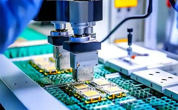
After solder paste printing and any required SPI inspection, the PCB enters the SMT pick-and-place machine.
According to the programmed component references, coordinates, and orientations, the machine picks components from tape feeders, trays, or other supply systems and places them accurately onto the PCB.
The components may include standard resistors and capacitors, as well as QFN, BGA, LGA, ICs, and various connectors.
In a conventional reflow process, the components are only held temporarily by the solder paste at this stage. They have not yet been permanently soldered to the PCB.
If an adhesive process is being used, the components are placed onto the adhesive dots instead.
Placement requires more than positional accuracy. The machine must also place the correct component with the correct orientation, polarity, and rotation angle. Missing components, incorrect parts, reversed polarity, or significant misalignment can affect both soldering quality and product functionality.
6. Adhesive Curing (Used in Specific Processes)
If adhesive was applied earlier, the components must be cured after placement.
A suitable curing or heating system is used to bring the adhesive to the required curing condition and secure the components to the PCB surface.
The purpose of the adhesive is only to hold the components in place. It does not provide the electrical connection.
The actual electrical and mechanical connections are still formed during the subsequent soldering process.
Therefore:
Adhesive dispensing → SMD placement → Adhesive curing → Wave soldering
is one specific SMT process route. It is not the standard process for modern reflow-based SMT production lines.
7. Reflow Soldering
PCBs assembled with solder paste enter a reflow oven after component placement.
The PCB passes through several temperature zones, typically including preheating, soaking, reflow, and cooling.
Once the temperature rises above the solder alloy’s liquidus temperature, the solder melts and wets the component terminals and PCB pads. As the board enters the cooling zone, the solder solidifies and forms stable solder joints.
At this stage, the components are finally connected to the PCB both electrically and mechanically.
A higher reflow temperature is not necessarily better. The actual process must take into account the solder paste type, PCB thermal mass, component temperature limits, and the distribution of components across the board. A suitable reflow profile usually needs to be developed and validated for each product.
How Is Soldering Quality Checked After Reflow?
Completing reflow soldering does not mean that assembly is finished.
The next step is usually to check for missing or misaligned components, soldering defects, and problems hidden underneath components.
AOI: Automated Optical Inspection
AOI uses cameras to capture images of the PCB and then evaluates the assembly and soldering condition according to programmed criteria.
It is commonly used to detect missing components, incorrect components, misalignment, incorrect orientation, polarity errors, tombstoning, and certain visible solder joint defects.
AOI is highly effective for visible defects, but it cannot inspect every solder joint.
For example, BGA solder balls are located underneath the package and cannot be directly observed using conventional optical inspection. Other inspection methods are required in such cases.
X-Ray Inspection
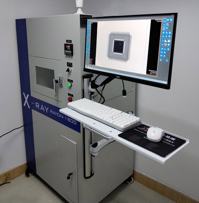
X-ray inspection is used to examine solder joints and internal areas that cannot be seen with standard optical equipment.
It is commonly used for bottom-terminated packages such as BGA, QFN, and LGA. X-ray inspection can help identify bridging, obvious solder ball abnormalities, voids, and other internal soldering issues.
However, not every PCB requires X-ray inspection. The decision usually depends on the component packages, product reliability requirements, and the manufacturer’s quality control plan.
Visual Inspection
Even as automated inspection equipment becomes more common, manual visual inspection still has practical value.
For prototypes, small production runs, or repaired PCBAs, engineers and operators may use magnifiers, microscopes, or digital microscopes to inspect solder joints, connectors, and specific assembly areas.
Certain mechanical or cosmetic issues may be easier to identify through manual inspection.
What Testing Is Required After SMT Assembly?
A PCBA may look fine externally and still fail to operate correctly.
After soldering and visual inspection, the board may therefore undergo ICT, flying probe testing, and FCT.
ICT: In-Circuit Test
ICT, or In-Circuit Test, uses test probes to contact designated test points on the PCB and check circuit nets and selected components.
Depending on the test program, ICT can detect open circuits, short circuits, resistance and capacitance values, and certain component parameters.
ICT generally requires a dedicated test fixture, making it more suitable for stable designs and higher-volume production.
Flying Probe Testing
Flying probe testing uses movable probes to contact test points on the PCB.
Unlike conventional ICT, it does not require a complete bed-of-nails fixture for each PCB design. This makes it suitable for prototypes, NPI, small production runs, and products that are frequently revised.
Flying probe testing offers greater flexibility, although its throughput is usually lower than ICT in high-volume production.
FCT: Functional Test
FCT, or Functional Circuit Test, focuses on whether the assembled PCBA operates as intended.
The test content depends on the product and may include power-up behavior, communication interfaces, inputs and outputs, sensor signals, displays, buttons, and driver circuits.
AOI, X-ray, ICT, and FCT identify different types of problems, so they are not simply interchangeable.
Does a PCB Always Need to Be Cleaned After Soldering?
Not necessarily.
Whether cleaning is required depends mainly on the flux type, the product’s cleanliness requirements, and its intended operating environment.
If cleaning is required, suitable equipment can be used to remove flux residues, ionic contaminants, and other manufacturing-related contamination.
If no-clean solder paste is used and the post-soldering residue meets the product requirements, a separate cleaning process may not be necessary.
For medical electronics, high-reliability products, or applications sensitive to ionic contamination, the decision should be based on the applicable standards and product requirements. The use of no-clean flux alone is not sufficient reason to automatically skip cleaning.
SMT Rework
If AOI, X-ray inspection, or electrical testing identifies a problem, the PCBA may need to undergo rework.
Common issues include component misalignment, missing or incorrect components, insufficient solder, bridging, and damaged components.
Standard solder joints can often be repaired using a soldering iron or hot-air rework tool. More complex packages, such as BGAs, generally require a dedicated rework station.
After rework, the board must undergo the appropriate inspection or testing again. Completing the repair without re-verification does not confirm that the problem has actually been resolved.
How Do Single-Sided, Double-Sided, and Mixed-Technology Assemblies Differ?
The process described above is a typical SMT production flow, but there is no single route that applies to every product.
The process changes according to the component layout and soldering method used on the PCB.
Single-Sided SMT Assembly
If SMD components are installed on only one side of the PCB, the process is usually straightforward:
Solder paste printing → SPI → SMD placement → Reflow soldering → AOI → X-ray inspection (if required) → Testing
This is one of the most common SMT process configurations.
Double-Sided SMT Assembly
Many PCBs have SMD components on both sides.
In this case, one side is printed, populated, and reflow-soldered first. The PCB is then flipped, and the corresponding processes are repeated for the other side.
The order in which the two sides are processed depends on factors such as component weight, package type, temperature sensitivity, and the PCB design.
Double-sided SMT does not necessarily require two separate production lines. The same SMT line can assemble both sides during separate production cycles.
Mixed SMT and THT Assembly
Some PCBs use both SMD components and THT components, such as connectors, transformers, large electrolytic capacitors, and other through-hole parts.
This is known as mixed-technology assembly.
A common approach is to complete SMT reflow soldering first and then install the THT components:
SMT reflow soldering → THT insertion → Wave soldering / Selective soldering / Hand soldering → Inspection and testing
If the solder side of the PCB also contains SMD components that are suitable for wave soldering, another process route may be used:
Adhesive dispensing → SMD placement → Adhesive curing → THT insertion → Wave soldering
In this case, wave soldering can solder some SMD terminals and THT leads at the same time.
However, not all SMD components are suitable for this method. Package type, component orientation, spacing, and pad design can all affect issues such as shadowing and bridging.
What Is the Difference Between Wave Soldering and Selective Soldering?
Wave soldering passes a relatively large area of the PCB’s solder side over a wave of molten solder. It is well suited to products with many THT components and layouts that support batch soldering.
Selective soldering applies solder only to specified THT joints or local areas. This allows it to avoid SMD components that have already been reflow-soldered, as well as other sensitive areas.
For products with a high mix of SMT and THT components or complex PCB layouts, selective soldering generally provides greater process flexibility.
Therefore, the presence of THT components on a PCB does not automatically mean that adhesive dispensing or wave soldering is required.
A More Complex SMT Process Is Not Always Better
SMT production involves many types of equipment and process steps, but not every project needs all of them.
A simple single-sided SMT PCB may only require:
Solder paste printing → SPI → Placement → Reflow soldering → AOI → Testing
A more complex PCBA containing BGAs, double-sided SMD components, and THT components may require additional X-ray inspection, a second reflow cycle, selective soldering, and more extensive electrical testing.
The right production process should be determined by the PCB design, component packages, production volume, reliability requirements, and test strategy—not by simply adding more equipment or inspection steps.
Conclusion
SMT may appear to be nothing more than “placing components on a PCB,” but it is actually a complete electronic assembly process.
Solder paste printing determines whether the correct amount of solder is deposited on each pad. The pick-and-place machine positions the components accurately. Reflow soldering forms the actual solder joints, while AOI, X-ray inspection, and electrical testing identify different types of defects.
When a PCB contains both SMD and THT components, the process becomes more varied. Adhesive dispensing, wave soldering, and selective soldering are not a fixed combination; they must be selected according to the component layout and the actual soldering requirements.
Do you need ISO 13485-compliant medical SMT assembly services? With 30 years of experience in PCB manufacturing and assembly, SugaMed provides one-stop services covering solder paste printing, precision component placement, reflow soldering, AOI, X-ray inspection, and functional testing. We prioritize quality control, batch traceability, and reliable delivery, offering customized solutions from prototypes and small-batch production to mass production based on your product requirements. Our goal is to help medical device manufacturers reduce manufacturing risks and improve product consistency.