
In SMT assembly, solder paste printing is a critical step before component placement. Solder paste must be transferred through the stencil and deposited accurately on the PCB pads. If the deposit volume is too low, the paste is misaligned, too much paste is applied, or adjacent deposits begin to connect, those problems can continue through placement and reflow and eventually become soldering defects.
Solder paste inspection (SPI) checks the condition of the printed paste before components are placed.
SPI is not a final product test, and it cannot determine whether a completed PCBA will function correctly. Its more precise role is early process control for solder paste printing.
By measuring the height, area, volume, position, and shape of paste deposits, SPI can detect printing variation while the pads are still exposed. This gives the manufacturing team an opportunity to address the problem early in the SMT process.
Table of contents
- What Is Solder Paste Inspection (SPI)?
- How Does 3D SPI Work?
- What Does 3D SPI Measure?
- Which Common Solder Paste Printing Defects Can SPI Detect?
- Why Inspect Solder Paste Before Component Placement?
- How Does SPI Data Help Control the Solder Paste Printing Process?
- What Determines Whether SPI Measurements Are Reliable?
- What Is the Difference Between 2D and 3D Solder Paste Inspection?
- Which PCB Assembly Projects Benefit Most from SPI?
- What Is the Difference Between SPI and AOI?
- How Do SPI, AOI, and X-Ray Divide Inspection Responsibilities in SMT?
- SPI Process Control for Medical Electronics PCBAs
- What Can SPI Not Tell You?
- Frequently Asked Questions About Solder Paste Inspection
- Conclusion
What Is Solder Paste Inspection (SPI)?
SPI is an automated optical measurement system used on an SMT assembly line to evaluate solder paste printing quality.
A typical SMT process can be summarized as follows:
Solder paste printing → SPI → Component placement → Reflow → AOI → Downstream testing
SPI is performed after solder paste printing and before component placement. At this stage, all paste deposits are still fully exposed, so the system can measure their geometry directly and compare the results with programmed process limits.
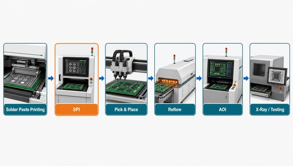
SPI answers practical questions about the printing process: Is the paste in the correct location? Is the deposited amount appropriate? Is thickness stable? Are there abnormal connections or shapes between adjacent pads?
It does not inspect component part numbers, polarity, post-reflow solder-joint quality, or circuit function. Those conditions require downstream methods such as AOI, X-ray, ICT, flying probe testing, or functional testing. For a broader view of these methods, see PCB assembly testing methods and their applications.
SPI should also not be confused with incoming inspection of solder paste material. Alloy composition, powder size, viscosity, solderability, and storage condition belong to material quality management. SPI evaluates the deposits that remain on PCB pads after the paste has been printed through the stencil.
How Does 3D SPI Work?
Most SPI systems used in modern SMT production rely on 3D optical measurement.
The equipment projects structured light or a defined optical pattern onto the PCB surface. Cameras capture information reflected from the paste, and software reconstructs a three-dimensional profile of each deposit.
The basic sequence is:
Optical projection → Image capture → 3D reconstruction → Geometric measurement → Comparison with programmed limits
Some 3D SPI systems use moiré-based or related structured-light techniques and collect height information from multiple angles. This helps reduce the effect of shadows and reflections on measurement results.
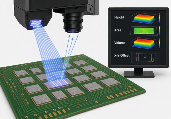
Compared with basic 2D image analysis, the main advantage of 3D measurement is that it can answer more than, “Is paste present here?” It can also answer, “How much paste is actually here?”
That distinction matters in SMT process control. From a top-down view, paste may appear to cover the correct pad area, but if its height is significantly below target, the total volume can still be insufficient. This type of condition is harder to identify reliably from a two-dimensional image alone.
What Does 3D SPI Measure?
SPI does more than take pictures. It measures the geometry of each solder paste deposit quantitatively.
| Measurement | What It Indicates |
|---|---|
| Height | Whether the paste deposit is too high or too low |
| Area | How much of the pad is covered by paste |
| Volume | The total amount of deposited solder paste |
| X/Y offset | The position of the deposit relative to the pad center |
| Shape | Whether the deposit edge, profile, or form is abnormal |
| Bridging | Whether adjacent paste deposits are connected |
| Smearing | Whether paste has spread, trailed, or contaminated nearby areas |
Volume is often one of the most useful process indicators because the amount of solder available to form a joint is directly related to the paste deposited during printing.
There is no single universal percentage limit that is appropriate for every PCB. Component package, land pattern, stencil thickness, aperture design, paste characteristics, and the validated process window all influence an acceptable deposit range. Inspection limits should therefore be established for the specific product and confirmed manufacturing process, rather than copied as one fixed number for every assembly.
Which Common Solder Paste Printing Defects Can SPI Detect?
The examples below illustrate the types of deposit conditions SPI is designed to distinguish before placement.
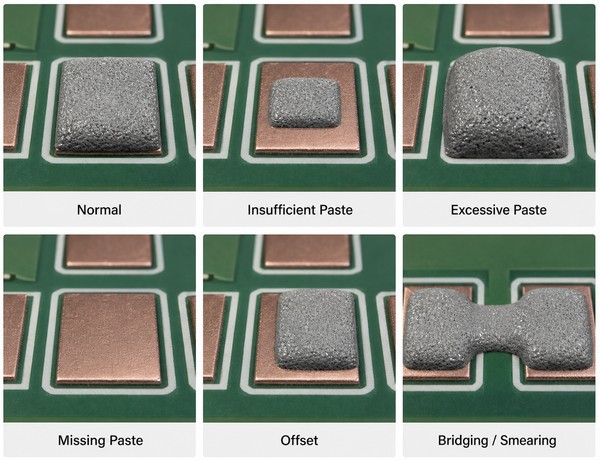
Insufficient solder paste
Insufficient paste is a common SPI finding. Possible causes include blocked stencil apertures, worn or damaged squeegees, incorrect printing pressure, inadequate stencil cleaning, or insufficient PCB support.
If it is not detected during printing, an insufficient deposit can increase the risk of too little solder or an open connection after reflow.
Excessive solder paste
More paste is not necessarily better. When paste volume is excessive, especially between closely spaced pads, the reflowed solder can have a higher risk of bridging or short circuits.
SPI is therefore used to identify not only insufficient deposits but also abnormal excess volume.
Missing solder paste
If an expected pad has no paste deposit, SPI can identify the condition before placement.
If the board proceeds to the next step, the component may still be placed correctly, but the affected termination will not have enough solder to form a reliable connection.
Solder paste offset
When the stencil and PCB are not aligned correctly, the deposit can shift in the X or Y direction relative to the pad.
Small offsets may be partly corrected by solder surface tension during reflow, but excessive displacement still increases the risk of soldering defects. SPI is not intended to predict whether reflow may compensate for the offset; its purpose is to determine whether the printing process itself remains stable and within its defined window.
Bridging and smearing
If paste deposits on adjacent pads already touch, SPI can flag a potential bridging condition.
Paste trails, distorted deposits, and irregular spreading can also be detected through shape and area data. These patterns are not merely reasons to reject the current board; they can also indicate that the printing process needs investigation.
Why Inspect Solder Paste Before Component Placement?
The greatest value of SPI is not simply that it adds another inspection step. Its value comes from finding variation early.
When a printing defect is detected immediately, the board has not yet gone through placement and reflow. The response can often follow a relatively simple path:
Detect the condition → Clean or reprint → Inspect again → Release to placement
If the same problem is not discovered, the board may continue through:
Placement → Reflow → AOI or X-ray → Soldering defect found → Rework
By then, components are already soldered to the PCB, so corrective action is more complex and rework cost is higher.
SPI therefore serves as an upstream process-control point. It helps the production line control printing before defects are carried into later assembly stages, instead of relying only on post-reflow inspection to screen defective boards.
How Does SPI Data Help Control the Solder Paste Printing Process?
The value of SPI should extend beyond a simple pass/fail decision.
If the same pads repeatedly show low paste volume, the important question is not only how to remove those boards from the line. The more useful question is why the same location continues to deviate.
By reviewing SPI data, manufacturing engineers can identify persistent trends in the printing process. Repeated insufficient paste in one area may point to blocked stencil apertures. A consistent X/Y shift across the board may indicate a stencil-to-PCB alignment problem.
If deposit measurements gradually change during a production run, the trend may indicate that the stencil-cleaning interval, squeegee condition, or printing parameters need attention.
SPI can therefore support the following control loop:
Measure → Detect variation → Identify the cause → Adjust the process → Verify again
On an SMT line with closed-loop capability, SPI data can also be linked to the solder paste printer so that the process can respond more quickly to printing variation.
What Determines Whether SPI Measurements Are Reliable?
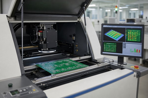
Owning a 3D SPI machine does not make every result automatically accurate. SPI is a measurement system, and its data must be sufficiently repeatable and stable.
Measurement repeatability is essential. If the same board produces substantially different results when measured several times, the data cannot reliably show whether the printing process is stable.
Calibration and program setup also affect results. The system must identify the correct pads and deposit regions, and inspection windows and thresholds must reflect the actual product and process.
A PCB is not a perfectly flat, optically uniform surface. Modern 3D SPI therefore also needs to manage board warpage, surface reflections, and the different optical behavior of materials and finishes.
Inspection sensitivity must be balanced as well. Limits that are too tight can create excessive false calls, while limits that are too broad may allow genuine defects to pass.
For projects with more demanding measurement-system requirements, methods such as gauge repeatability and reproducibility (GR&R) can be used to evaluate measurement repeatability and reproducibility.
What Is the Difference Between 2D and 3D Solder Paste Inspection?
Earlier or simpler SPI systems may rely mainly on two-dimensional image analysis. 2D SPI mainly provides planar data such as deposit area, position, and appearance.
Solder paste, however, has height. Two deposits can cover nearly the same area when viewed from above yet contain very different volumes.
3D SPI adds height measurement to area data and calculates volume, creating a more complete description of the actual deposit.
For example, a deposit may appear to cover the pad correctly but reach only a fraction of its expected height. A 2D image may not represent the true paste quantity accurately, while 3D SPI can identify the difference more directly through volume data.
This is one reason 3D SPI is widely used in modern SMT production.
Which PCB Assembly Projects Benefit Most from SPI?
SPI is not limited to assemblies that are considered complex. However, its process data becomes especially valuable as the SMT process window narrows.
Fine-pitch and high-density assembly
As components, pads, and pitch become smaller, the tolerance available for stencil apertures and paste deposits also decreases.
Small passive packages such as 0201 and 01005, along with dense IC lead patterns, generally require tighter printing consistency. In these situations, small volume or positional variations can have a greater effect on downstream soldering results.
BGA, QFN, and LGA packages
The roles of SPI and X-ray need to be distinguished clearly for bottom-terminated packages.
SPI cannot inspect reflowed BGA solder joints because it runs before the BGA is placed. Its contribution is to verify the paste deposits on BGA, QFN, or LGA pads before placement. BGA assembly then continues through placement and reflow.
After the component has been placed and reflowed, hidden solder joints may require X-ray inspection. SPI checks pre-reflow solder paste; X-ray examines hidden joints after reflow. They solve different problems.
NPI and new PCB revisions
SPI is particularly useful during new product introduction (NPI).
When a new product enters SMT production for the first time, the manufacturing team must confirm more than whether the board can be assembled once. It needs to determine whether the printing process can be repeated consistently.
SPI data can help the engineering team evaluate whether stencil apertures, PCB support, alignment, and print settings produce a stable process window. If a region shows repeated variation during the initial build, the issue can often be addressed while the design or process is still relatively easy to change.
This is usually more effective than correcting recurring defects after the product has entered routine production.
What Is the Difference Between SPI and AOI?
SPI and AOI are both common automated optical inspection technologies in SMT, so they are sometimes confused. In practice, they inspect different stages of production.
| SPI | AOI |
|---|---|
| Performed after solder paste printing | Usually performed after placement or reflow |
| Inspects solder paste deposits | Inspects components and visible soldering conditions |
| Pads are still uncovered | Components are already installed on the PCB |
| Focuses on the printing process | Focuses on assembly results |
| Measures paste height, area, and volume | Checks missing or incorrect components, offset, polarity, and visible solder joints |
SPI does not replace AOI, and AOI does not fully replace SPI. Once components cover the pads, AOI cannot recover the original solder paste deposit data from the printing stage.
The two methods work best as complementary controls: SPI controls the printing process, while AOI evaluates subsequent assembly results.
How Do SPI, AOI, and X-Ray Divide Inspection Responsibilities in SMT?
Their roles become clearer when placed in sequence:
Solder paste printing → SPI checks paste deposits → Component placement → Reflow → AOI checks components and visible soldering defects → X-ray checks selected hidden solder joints
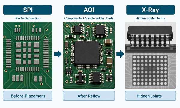
These technologies are not competing alternatives. They observe different stages of SMT manufacturing and different defect types.
If the assembly also requires verification of electrical connectivity and actual operation, the quality plan may add flying probe testing, ICT, or functional testing. The appropriate combination depends on product design, risk, production volume, and customer requirements.
SPI Process Control for Medical Electronics PCBAs
There is no separate category of SPI technology used only for medical electronics. Patient monitors, infusion systems, respiratory devices, and other medical electronics use the same fundamental SMT printing and SPI measurement technologies as other assemblies.
What changes is the project complexity and the required level of process control. When a medical PCB assembly includes fine-pitch ICs, small passives, BGA or QFN packages, or high component density, stable paste deposition and careful confirmation of print parameters during NPI become more important.
For projects produced under a controlled quality system, SPI also involves more than completing an automated inspection cycle. The project may require controlled process parameters, PCB revision management, inspection-program version control, nonconformance records, lot or serial-number traceability, and retention of inspection data.
Within an ISO 13485 quality management system, applicable production and inspection processes are controlled according to customer requirements, product risk, internal procedures, and project-specific quality requirements.
ISO 13485 itself does not prescribe one particular SPI machine for every medical PCBA. Whether SPI is used, how its limits are defined, and how its data supports process control must still be determined for the specific product and manufacturing flow.
What Can SPI Not Tell You?
SPI is important, but its inspection scope is specific.
It cannot determine whether the wrong component has been placed or whether component polarity is correct. It cannot inspect a reflowed BGA joint hidden beneath the package, test a circuit for opens or shorts, or demonstrate that the PCBA functions correctly after power-up.
A complete PCB assembly quality plan therefore usually combines several methods:
- SPI: Is the solder paste printing condition acceptable?
- AOI: Are components and visible soldering conditions acceptable?
- X-ray: Do hidden solder joints show internal anomalies?
- Flying probe or ICT: Do circuit connections and selected electrical parameters meet requirements?
- FCT: Does the powered PCBA perform its defined functions?
Understanding these boundaries is more useful than asking which single inspection technology is “best.”
Frequently Asked Questions About Solder Paste Inspection
What does SPI mean in PCB assembly?
SPI stands for solder paste inspection. It is normally performed after solder paste printing and before component placement to measure the condition of deposits on PCB pads.
What does 3D SPI measure?
3D SPI typically measures paste height, area, volume, X/Y offset, and shape. It can identify conditions such as insufficient paste, excessive paste, missing deposits, misalignment, bridging, and smearing.
Which defects can SPI detect?
Common inspection targets include insufficient paste, excessive paste, missing paste, print offset, bridging, and abnormal deposit shape. The exact items and acceptance limits must be defined in the product-specific inspection program.
What is the difference between SPI and AOI?
SPI primarily evaluates solder paste before reflow. AOI primarily evaluates component position, polarity, and visible soldering conditions after placement or reflow. SPI focuses on printing; AOI focuses on assembly results.
Can SPI inspect BGA solder joints?
No. SPI is performed before the BGA is placed, so it measures paste on the BGA pads rather than completed solder joints. After reflow, hidden BGA joints are generally evaluated with X-ray when inspection is required.
Conclusion
The value of solder paste inspection goes beyond rejecting a PCB with a poor print. SPI allows an SMT manufacturing team to see what is happening in the printing process before components are placed and reflowed.
By measuring deposit height, area, volume, position, and shape, SPI can identify printing variation early and help engineers determine whether the stencil, alignment, cleaning condition, or print settings need adjustment.
Its most accurate role is that of a solder paste printing process-control tool.
SPI does not replace AOI, X-ray, electrical testing, or functional testing. Each method addresses a different risk in PCB assembly. For stable volume production, high-density SMT, NPI, and electronics that require disciplined process control, the important capability is not simply owning an SPI machine. It is using reliable SPI data to detect process variation and respond before that variation moves into downstream assembly.