
A medical PCB is a printed circuit board used in a medical device or healthcare electronic system. It may remain a bare board or become part of a medical PCB assembly after components are mounted and tested. Medical PCBs are used in patient monitors, ECG devices, pulse oximeters, diagnostic instruments, infusion pumps, portable ultrasound systems, and wearable medical devices.
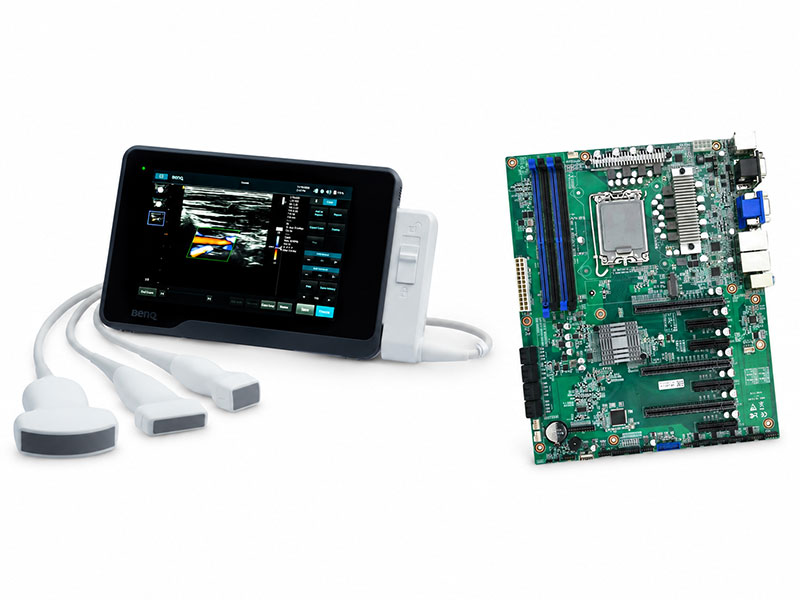
No single laminate, layer count, surface finish, or IPC class defines a universal “medical-grade PCB.” Medical describes the application context, not one standardized PCB construction.
The right PCB construction depends on what the board is expected to do inside the device. A board that handles weak ECG signals may place greater emphasis on noise control, grounding, and signal integrity. A compact wearable device may be more constrained by board size and interconnect density. Designs involving patient connections or safety-related circuits may also need specific isolation structures and layout controls derived from system-level safety requirements.
The more useful design question is:
What must this PCB do inside the medical device, and which electrical, mechanical, manufacturing, and regulatory risks need to be controlled?
Key Features of Medical PCBs
Medical devices vary widely, so their PCB requirements vary as well. Even so, several engineering concerns tend to receive more attention in medical electronics than in typical consumer products.
Reliability and Repeatability
Reliability is not limited to whether the first prototype works.
Materials, stack-up, via structures, surface finishes, and other critical manufacturing conditions need to remain consistent as a project moves from prototype to repeat production. Later production lots should continue to reflect the approved design and material requirements.
This is one reason revision control, change control, and traceability are important in medical electronics manufacturing.
For example, replacing a PCB laminate with another material that appears “similar” on paper may still require review. Changes in Tg, CTE, CAF resistance, impedance behavior, or processing characteristics could affect the product or invalidate assumptions made during earlier verification.
Signal Integrity and Noise Control
Many medical devices process very small analog signals.
ECG, SpO₂, sensor interfaces, and measurement systems may combine analog circuitry, power conversion, digital processing, and communications on the same board. Functional partitioning, return paths, reference planes, decoupling, and stack-up design can all influence signal quality.
There is no universal medical PCB layout rule for these circuits.
The board should be designed around the actual AFE, ADC, MCU, communication devices, and system architecture rather than relying on simplified rules such as always separating analog and digital grounds.
Miniaturization and Interconnect Density
Portable, handheld, and wearable medical devices often need to fit sensing, processing, wireless communication, and power management into a limited space.
HDI becomes useful when conventional through-hole multilayer construction can no longer support efficient BGA fan-out or dense routing.
Microvias, blind and buried vias, via-in-pad, and sequential build-up structures can increase routing density. They also create tighter relationships between stack-up design, via structure, materials, and manufacturing capability.
For that reason, HDI should be selected when the interconnect density justifies it, rather than simply because the board is intended for a medical product.
Manufacturing and Product Traceability
Medical electronics projects often require stronger links between production records and the hardware being built.
Useful traceability goes beyond a generic claim of “full traceability.”
Depending on the project, records may link the production lot, PCB manufacturing lot, critical component lots, PCBA serial number, firmware version, test procedure revision, and inspection or test status.
When a field issue occurs, these records can help answer practical questions:
Which units are affected? Which materials and components were used? Which firmware and test revision were applied?
That level of traceability can be more valuable than simply adding another final inspection.
Common Types of Medical PCBs
Medical devices can use nearly every major PCB construction. The appropriate choice depends on space, interconnect density, mechanical requirements, signal performance, and reliability needs.
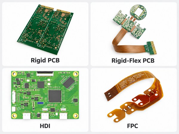
Rigid PCB
Rigid PCBs are widely used throughout medical electronics.
Patient-monitoring equipment, diagnostic instruments, power-control systems, therapeutic devices, and general control boards may all use rigid multilayer construction.
When the board is mounted in a fixed mechanical structure and does not need to flex, a conventional rigid multilayer PCB is often the most practical option.
As circuit complexity increases, additional signal, power, and reference layers can be added to support routing, impedance control, power integrity, and EMI performance.
Flex PCB
Flexible PCBs use flexible dielectric materials, allowing the circuit to bend or connect electronic sections within limited spaces.
They can be useful where space is restricted, where static or dynamic flexing is required, or where traditional wiring harnesses are difficult to package.
Wearable medical electronics, sensor assemblies, and other compact devices may use flex circuits to reduce separate connectors and wiring.
Flexibility, however, does not automatically make a design more reliable. Bend areas, copper construction, coverlay, bend radius, and assembly handling all need to match the actual mechanical environment.
Rigid-Flex PCB
Rigid-flex PCBs combine rigid component-mounting areas with flexible interconnect sections.
Components can be assembled on the rigid portions while the flex sections connect different board areas or accommodate three-dimensional packaging.
This construction can reduce board-to-board connectors and separate wiring in wearable products, portable equipment, and other space-constrained medical devices.
SugaMed supports flex and rigid-flex PCB fabrication and assembly for wearable, portable, and other compact medical electronics.
HDI PCB
HDI primarily addresses interconnect density.
It can be useful when a design includes dense BGA fan-out, fine-pitch components, microvias, via-in-pad, or routing requirements that cannot be handled efficiently with conventional through-hole construction.
SugaMed currently supports 1+N+1, 2+N+2, and 3+N+3 HDI structures, along with blind vias, buried vias, and via-in-pad, subject to project review.
When a standard multilayer PCB already provides enough routing space, adding HDI can introduce unnecessary manufacturing complexity.
What Materials Are Used in Medical PCBs
There is no universal “medical-grade laminate.”
Material selection should reflect the board’s operating temperature, thermal cycling, electrical performance, mechanical requirements, signal frequency, interconnect structure, and manufacturing process.
FR-4 and High-Tg FR-4
FR-4 remains a common material system for medical electronics.
For many designs with moderate operating temperatures, frequencies, and structural requirements, an appropriate FR-4 grade is sufficient.
High-Tg FR-4 may be considered when the board is exposed to higher processing temperatures, repeated reflow cycles, demanding thermal cycling, or other conditions that require greater thermal stability.
“High Tg,” however, is still only one material characteristic.
When laminate performance is important, the actual material grade should be reviewed together with properties such as Tg, Td, CTE, and CAF resistance.
Polyimide
Polyimide is widely used in Flex and Rigid-Flex construction.
Its thermal and mechanical characteristics make it suitable for flexible structures used in wearable devices, sensors, and other compact medical electronics.
The final material construction should still be selected around the required bending behavior, copper type, flex geometry, and assembly process.
RF and Low-Loss Materials
Some medical devices include wireless communication, RF sensing, imaging functions, or other high-frequency circuitry where conventional FR-4 may not provide the required electrical performance.
These designs may use PTFE, hydrocarbon ceramic, Rogers-type materials, or other low-loss material systems.
A laminate should not be selected by comparing a single Dk value.
Dk, Df, copper roughness, dielectric thickness, stack-up, trace geometry, and manufacturing tolerance all contribute to impedance and insertion loss.
Specialized Materials
Certain medical electronics may also use ceramic, metal-core, or other specialized substrates.
These materials are chosen to solve specific thermal, electrical, or mechanical problems rather than simply to obtain a “higher-grade” board.
SugaMed’s current PCB manufacturing range includes FR-4, High-Tg FR-4, polyimide, rigid-flex material systems, PTFE and RF materials, and other specialized substrates subject to project review.
Medical PCB Design Considerations
Many PCB reliability issues are influenced by design decisions made before manufacturing begins.
Electrical Safety and Isolation
In medical electrical equipment, isolation structures, creepage, clearance, and material selection may be important parts of the safety design.
There is no universal creepage distance or hipot requirement for every medical PCB.
The applicable values may depend on working voltage, MOP, MOOP or MOPP, material group, pollution degree, altitude, applied-part classification, and the standards that apply to the finished device.
For the PCB manufacturer, one of the most important responsibilities is maintaining approved safety-critical geometry.
If a DFM proposal changes an isolation slot, critical spacing, or another safety-related feature, the change should be reviewed with the design team rather than treated as a routine manufacturing adjustment.
Signal Integrity and EMC
A medical PCB may include low-level analog signals, high-speed digital interfaces, power circuitry, and wireless communication on the same board.
Reference planes, return paths, controlled impedance, power distribution, component placement, grounding, and EMI should be considered according to the actual circuit.
Controlled impedance is not automatically required simply because a board is used in a medical device, and there is no universal stack-up for medical electronics.
These requirements should come from the circuit and system design.
Thermal Management
Thermal management matters even when the device is not considered a high-power product.
DC/DC converters, processors, LED drivers, motor drivers, charging circuits, and other components can create localized hot spots on compact boards.
Copper distribution, thermal vias, stack-up, component placement, and enclosure design often need to be considered together.
High-Tg material can improve material stability in certain high-temperature and thermal-cycling conditions, but it is only one part of a thermal design strategy.
Design for Manufacturing and Testing
A PCB must be more than electrically correct in the design software. It also needs to be practical to fabricate, assemble, and test consistently.
A manufacturing review may consider stack-up, via structure, trace and space, surface finish, panelization, fiducials, component clearance, thermal pads, test-point accessibility, and consistency between PCB and assembly data.
Early review becomes especially valuable for designs that use BGA, QFN, HDI, or rigid-flex construction. A structured PCB assembly DFM checklist can also reduce revision conflicts and missing manufacturing data before quotation or NPI.
How Are Medical PCBs Manufactured and Inspected
The fundamental manufacturing processes used for medical PCBs are similar to those used for other high-reliability printed circuit boards.
A typical multilayer board may still go through inner-layer imaging, etching, AOI, lamination, drilling, hole metallization, outer-layer processing, solder mask, surface finishing, routing, and electrical testing.
The key difference is usually the level of control applied to materials, revisions, critical processes, and acceptance requirements.
PCB Fabrication
Before fabrication begins, the manufacturing data should be clearly defined and controlled.
That may include the stack-up, material, copper weight, drill data, via structure, impedance requirements, surface finish, dimensions, tolerances, and electrical-test requirements.
CAM engineering can improve manufacturability, but it should not change the original design intent without approval.
Any proposed change that affects impedance, via construction, critical spacing, materials, or other controlled requirements should be reviewed before production.
Bare PCB Inspection
No single inspection method can detect every PCB defect.
AOI can identify many pattern-related defects and visible anomalies. Electrical testing checks specified networks for opens and shorts. Microsection analysis can be used to examine plating and internal structures. Controlled-impedance boards may also require impedance verification.
The inspection plan should reflect the actual risks and purchase requirements of the project instead of assuming every medical PCB needs the maximum possible level of inspection.
From PCB to PCBA
Once the project moves into assembly, the number of controlled variables increases.
The focus expands from the bare PCB to the BOM, component sourcing, solder paste printing, placement, reflow, THT, programming, AOI, X-Ray, ICT, and functional testing.
Each inspection method covers a different type of risk.
AOI is effective for visible components and solder joints, but it cannot directly inspect solder joints beneath a BGA. X-Ray is better suited to hidden joints under BGA, QFN, and other bottom-terminated packages. ICT and FCT address different electrical and functional requirements.
A sound test strategy starts with the potential failure modes and then selects the inspection methods that can actually detect them.
Under SugaMed’s current PCB assembly inspection and testing coverage, prototype SMT assemblies receive 100% post-reflow AOI, and BGA solder joints receive 100% X-ray inspection. Coverage for QFN, LGA, and other bottom-terminated packages is defined by package type, project risk, and customer requirements.
That is more meaningful than a broad “100% inspection” claim because it explains what is being inspected and why.
What Standards Are Relevant to Medical PCBs
ISO, FDA, IEC, and IPC references often appear together in medical PCB discussions, but they serve different purposes.
ISO 13485
ISO 13485:2016 is a quality management system standard for organizations involved in medical devices and related services.
It addresses how an organization operates within a controlled quality system. It does not prescribe a specific PCB material, layer count, or IPC class.
SugaMed operates an ISO 13485 medical PCB manufacturing and assembly system for applicable medical electronics projects. Certification describes the quality system and its scope; it does not certify an individual bare PCB as a medical device.
ISO 14971
ISO 14971:2019 provides a risk-management framework for medical devices.
It can help the OEM determine which PCB or PCBA characteristics require additional controls based on product risk. It is not a PCB manufacturing specification.
IEC 60601-1
IEC 60601-1 addresses basic safety and essential performance for medical electrical equipment.
Some of its device-level requirements can influence PCB isolation, layout, materials, and safety-critical components.
A bare PCB should therefore not be marketed simply as an “IEC 60601-certified PCB.”
IPC Standards
IPC standards cover multiple aspects of PCB design, fabrication, acceptability, assembly, and soldering.
The applicable standards and acceptance criteria should be defined according to the product, customer requirements, reliability needs, and contract.
Medical electronics are not automatically required to use IPC Class 3.
Some projects may be appropriately built to Class 2, while higher-reliability applications may specify Class 3 or additional customer-specific acceptance criteria.
FDA QMSR
Products intended for the U.S. medical device market may also fall within the FDA Quality Management System Regulation.
The FDA Quality Management System Regulation became effective on February 2, 2026 and incorporates ISO 13485:2016 into the revised U.S. quality-system framework.
Regulatory responsibility still depends on the role of the finished-device manufacturer and other parties in the supply chain. A PCB or PCBA supplier should not be described as an “FDA-approved PCB manufacturer” simply because it supports medical projects.
Where Are Medical PCBs Used
Medical PCBs are used across a wide range of healthcare electronics, and the same PCB technology can serve very different types of devices.
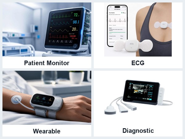
Patient Monitoring Equipment
Patient monitors, ECG monitors, ECG patches, pulse oximeters, blood pressure monitors, and other patient-monitoring systems all rely on PCB or PCBA assemblies.
Some of these products focus on low-level signal acquisition, while others combine sensing with displays, communication, power management, and multiple peripheral interfaces.
For device-specific manufacturing considerations, see SugaMed’s pages for Patient Monitor PCBA, ECG Patch PCBA, Pulse Oximeter PCBA, and Blood Pressure Monitor PCBA.
Diagnostic and Laboratory Equipment
Medical PCBs are also used in glucose meters, PCR systems, hematology analyzers, biochemistry analyzers, immunoassay equipment, and other IVD and laboratory electronics.
These systems may combine precision analog measurement, motion control, temperature regulation, power electronics, and digital communication.
Therapeutic and Respiratory Devices
Infusion pumps, CPAP/BiPAP systems, nebulizers, TENS/EMS devices, and AEDs also depend on PCB and PCBA assemblies.
The board-level priorities vary by product. One design may focus on motor control and sensor feedback, while another may place greater emphasis on power management or electrical stimulation.
Medical Imaging and Portable Equipment
Portable ultrasound systems and similar equipment may combine high-speed data, dense component placement, controlled impedance, and tight mechanical constraints.
HDI, fine-pitch fabrication, and more complex stack-ups become useful when routing density or signal requirements genuinely call for them.
Wearable and Home-Use Medical Devices
Wearable and home-use medical electronics often need to balance compact size, low power consumption, wireless communication, battery operation, and mechanical constraints.
Those requirements can make Flex, Rigid-Flex, or HDI an appropriate choice for certain designs.
Medical PCB vs. Standard Commercial PCB
Medical PCBs and standard commercial PCBs share many of the same fundamental manufacturing technologies.
The differences below reflect common project priorities rather than strict industry boundaries. Automotive, aerospace, industrial-control, and other high-reliability electronics may use similarly rigorous controls.
| Area | Typical Commercial PCB Project | Common Medical PCB Priority |
|---|---|---|
| Materials | Selected around cost and performance | Greater emphasis on consistency with approved materials and device requirements |
| PCB structure | Defined by circuit and mechanical needs | Also project-specific; there is no universal “medical” construction |
| Acceptance criteria | Defined by the purchase specification | Often linked more closely to intended use, risk, and customer requirements |
| Traceability | Applied as needed | Often places more emphasis on lot, revision, and manufacturing-record linkage |
| Change control | Depends on the project | Material, revision, and process changes may require tighter control |
| Inspection and testing | Balanced against cost and risk | Greater emphasis on matching inspection coverage to potential failure modes |
| Documentation | Based on product and customer needs | May require more complete production, inspection, test, and revision records |
The practical question is not:
“How many levels higher is a medical PCB than a standard PCB?”
It is:
“What function does this PCB perform in the medical device, and what design and manufacturing controls are needed to keep that function reliable?”
Choosing the Right Medical PCB for Your Project
There is no universal PCB configuration for medical electronics.
An ECG wearable may benefit from Rigid-Flex construction and low-noise signal design. A large diagnostic instrument may work well with a conventional multilayer rigid PCB. A compact handheld product may require HDI. A device with RF communication may need low-loss materials.
Before selecting the PCB construction, it is useful to define the device function and operating environment, PCB size and mechanical constraints, major component packages and routing density, signal and RF requirements, thermal conditions, expected production volume and product life, and the required inspection, testing, and traceability strategy.
That information gives a manufacturer far more useful direction than simply requesting a “medical-grade PCB.”
SugaMed supports medical electronics projects from PCB engineering review and fabrication through component sourcing, assembly, inspection, and testing. If Gerber files, stack-up information, a BOM, or preliminary design data are available, the engineering team can review whether rigid, flex or rigid-flex, HDI, High-Tg, RF, or another PCB technology is appropriate for the actual requirements.
A well-designed medical PCB is not the one with the highest possible specification. It is the one whose design, materials, manufacturing controls, and verification are appropriate for the device in which it will be used—and can remain consistent from prototype through repeat production.