
A completed electronic assembly consists of a bare printed circuit board and the electronic components mounted on it. The PCB provides mechanical support and copper interconnections, while resistors, capacitors, inductors, diodes, transistors, integrated circuits, and connectors perform the board’s electrical functions. Modern PCB assembly therefore depends on both the circuit board design and the package and mounting requirements of every component in the bill of materials.
Most small electronic components used in phones, computers, automotive electronics, and medical devices are now installed by surface-mount technology. This article explains what SMT components are, why they support compact automated assembly, how they are classified, which package families are common, and where through-hole technology still remains useful.
What Is an SMT Component
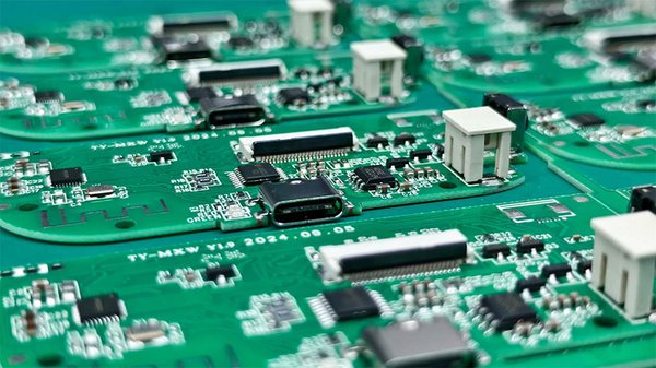
An SMT component is an electronic component designed to be mounted directly on pads on the surface of a PCB. In surface-mount assembly, solder paste is deposited on the pads, the component is placed by automated equipment, and the solder is melted in a controlled reflow process to form the electrical and mechanical connection.
The most visible difference from through-hole assembly is the mounting method. Through-hole components normally have leads that pass through drilled and plated holes before they are soldered on the opposite side. SMT components do not require their terminals to pass through the board. Their terminations connect directly to surface pads.
SMT describes the assembly process. SMD, or surface-mount device, describes a component intended for that process. Some older references use SMC mainly for passive surface-mount components and SMD for active devices, but current industry usage often applies SMD broadly to chip resistors, capacitors, diodes, transistors, and ICs. The practical question is whether the package is designed for surface mounting, not which of these abbreviations a supplier prefers.
Why Are SMT Components Getting Smaller
One of the main reasons SMT developed was to reduce the board area consumed by component bodies, leads, and mounting holes. A traditional dual in-line package commonly uses a 2.54 mm lead pitch. Modern surface-mount ICs may use pitches of 0.5 mm, 0.4 mm, or approximately 0.3 mm, depending on the package family and device.
The change is even more apparent in rectangular chip components. An EIA 1206 resistor or capacitor is approximately 3.2 mm by 1.6 mm. Common smaller formats include 0402 at about 1.0 mm by 0.5 mm, 0201 at about 0.6 mm by 0.3 mm, and 01005 at about 0.4 mm by 0.2 mm. Package dimensions and tolerances must always be confirmed in the component manufacturer’s data sheet.
Smaller components allow more circuitry to fit within the same PCB outline. This does not only make the finished product smaller. In space-constrained products, reducing component area can leave more room for batteries, antennas, sensors, connectors, thermal structures, or mechanical supports. The tradeoff is that smaller terminations and tighter spacing require more precise land patterns, stencil apertures, printing, placement, and inspection.
Most SMT Components Have Short or No External Leads
Many SMT components do not have conventional wire leads. Chip resistors and multilayer ceramic capacitors normally use metallized end terminations. BGA packages use solder balls on the bottom of the package. QFN and LGA packages use terminals or lands located mainly underneath the component body.
Other packages, including SOIC, TSSOP, QFP, and SOT, still have visible external leads, but the leads are short and connect to surface pads. Shorter interconnections can reduce the electrical path length and some package-related parasitic inductance and capacitance, which can support compact high-frequency and high-speed layouts. Actual performance still depends on the device, package construction, PCB stackup, routing, return paths, and operating frequency. An SMT package is not automatically superior in every electrical application.
How SMT Increases PCB Assembly Density
A through-hole component needs drilled holes, plated barrels, annular rings, and clearances around its leads. SMT components are mounted on surface pads, so designers can use the board area and internal routing space more efficiently. Components may also be assembled on both sides of a PCB when the design and manufacturing process support double-sided SMT.
These advantages make higher component density possible, but density should not be increased without considering manufacturability. Placement clearances, rework access, solder-joint geometry, thermal behavior, test access, and inspection capability still have to be included in the layout.
Why SMT Components Support Automated Assembly
Most SMT components are supplied in standardized tape-and-reel, tray, or tube packaging. Pick-and-place equipment can feed each part, identify its orientation, correct its position, and place it on the programmed PCB location. This makes SMT well suited to repeatable automated production.
A typical process sequence is solder paste printing followed by solder paste inspection, component placement, reflow soldering, and automated optical inspection. The exact sequence can include additional steps depending on the board, package types, production volume, and agreed test plan.
For a PCBA containing hundreds or thousands of placements, automated feeding and placement are far more practical than inserting every component manually. This is why SMT is the primary assembly technology for most modern electronic products, even though selected connectors, transformers, relays, and other components may still use through-hole mounting.
What Types of SMT Components Are There
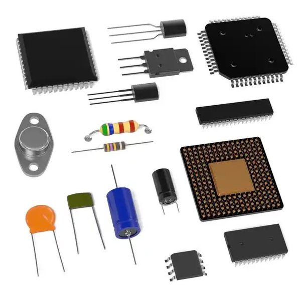
SMT components can be classified by electrical function, package shape, construction, or application. A practical functional classification divides them into passive components, active devices, and electromechanical components.
Passive SMT Components
The most common passive SMT components are chip resistors, multilayer ceramic capacitors, tantalum capacitors, chip inductors, ferrite beads, thermistors, and varistors. Passive components often account for the highest placement count on a PCBA, even when the board contains only a few major ICs.
Rectangular chip packages are widely used, but passive components are not limited to that shape. Surface-mount aluminum electrolytic capacitors, trimmers, crystal units, transformers, filters, and larger inductors may use cylindrical, molded, shielded, or other specialized constructions. Resistor arrays, capacitor arrays, and integrated filters can combine several elements in one package to reduce placement count and board area.
Active SMT Devices
Active SMT devices include diodes, transistors, power semiconductors, and integrated circuits. Their packages vary widely because different devices require different numbers of connections, thermal paths, electrical characteristics, and board areas. Small-signal transistors often use SOT packages, many diodes use SOD packages, and integrated circuits may use SOIC, TSSOP, QFP, QFN, BGA, CSP, and related package families.
QFP distributes leads around four sides of the package and can provide many visible I/O connections. BGA places an array of solder balls beneath the package, allowing a high connection count within a compact outline. CSP aims to keep the package dimensions close to the die size. Each approach balances size, I/O count, electrical and thermal performance, assembly capability, inspection, rework, availability, and cost.
Electromechanical SMT Components
Surface mounting is also used for relays, switches, connectors, filters, sensors, and other electromechanical parts. These components are often larger and mechanically more complex than chip passives or ICs.
A connector that will experience repeated mating force or external mechanical stress may need through-hole retention posts, additional board locks, or a fully through-hole mounting arrangement. Many PCBAs therefore use mixed SMT and through-hole construction rather than forcing every component into one mounting technology.
What Are the Most Common SMT Package Types
Package abbreviations appear throughout PCB bills of materials, component data sheets, and footprint libraries. Common families include the following:
- Chip packages: Two-terminal rectangular packages widely used for resistors, capacitors, inductors, ferrite beads, and related passive components.
- SOT and SOD: Small-outline transistor and diode packages used for discrete semiconductors and some compact ICs.
- SOIC and TSSOP: Gull-wing leaded packages with terminals on two sides. TSSOP is generally thinner and uses tighter lead spacing than standard SOIC formats.
- QFP: A gull-wing package with leads on four sides, often used for microcontrollers, processors, and control ICs.
- QFN: A leadless or nearly leadless package with terminals around the underside perimeter and, in many designs, an exposed thermal pad.
- BGA: A package with an array of solder balls on its underside. The hidden connections require process control and an appropriate inspection plan. Detailed requirements should be reviewed as part of BGA assembly.
- CSP: A compact package whose outline is close to the size of the semiconductor die, used where board area and package height are tightly constrained.
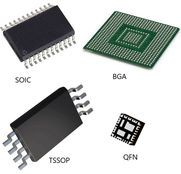
Packages that are all classified as SMT can still require very different pad designs, stencil apertures, placement accuracy, reflow conditions, inspection methods, and rework skills. QFP leads are externally visible and can often be evaluated by AOI. BGA solder joints are hidden underneath the package and normally require X-ray inspection for structural assessment. QFN and LGA inspection requirements depend on the package structure, assembly risk, PCB design, and project-specific plan.
What Are the Limitations of SMT Components
SMT is mature and widely used, but it does not replace through-hole technology in every application. Mechanical loading is a common reason to retain through-hole features. Large connectors, transformers, terminal blocks, and components exposed to insertion force, vibration, or cable load may need stronger board retention than surface pads alone can provide.
Inspection and rework can also be more difficult. The solder joints of BGA, LGA, and many QFN packages are partly or completely obscured by the component body. Optical inspection cannot fully evaluate those hidden interfaces, and replacing the device usually requires controlled rework equipment and trained personnel.
As component size and pitch decrease, the process window becomes more demanding. Land-pattern accuracy, stencil design, solder paste transfer, PCB support, placement alignment, reflow profile, moisture handling, and inspection all become more important. The appropriate methods should be defined through PCB assembly inspection and testing rather than assuming that one inspection method is sufficient for every package.
Hermetic and Nonhermetic SMT Packages
Some references also classify component packages as hermetic or nonhermetic. Most SMT devices used in consumer and industrial electronics have nonhermetic plastic or resin-based packages. Certain aerospace, defense, high-reliability instrumentation, or specialized industrial applications may use ceramic or metal hermetic packages to provide a stronger barrier between the internal device and moisture or contaminants.
Hermetic construction does not by itself define the component’s allowable operating temperature. Temperature range, storage conditions, moisture sensitivity, reflow limits, and reliability qualifications must be checked in the manufacturer’s data sheet and the requirements for the actual product.
Conclusion
An SMT component is not one specific electronic part. It is any component packaged for direct mounting on PCB surface pads. Resistors, capacitors, inductors, diodes, transistors, ICs, relays, switches, and connectors can all be supplied in surface-mount forms.
SMT packages reduce or eliminate long leads and component mounting holes, which supports compact layouts, higher placement density, double-sided assembly, and automated production. These benefits come with tighter requirements for footprint design, paste printing, placement, reflow, inspection, and rework as package size and pitch decrease.
In practical PCBAs, SMT and THT are complementary. The correct choice depends on the component package, electrical performance, mechanical loading, thermal behavior, manufacturing capability, inspection access, service requirements, and the design objectives of the finished product.