
Designing a rigid-flex board starts with a sequence of decisions, not a layer stack. Before routing a single trace, you need to know how the board will bend, where the rigid and flex material actually meet, and what the fabricator needs to see on the mechanical drawing to build it correctly. Skipping that sequence is why rigid-flex designs tend to come back from DFM review with structural changes rather than minor comments — the layout was finished before the mechanical decisions were.
This guide walks through that decision order: bend type, zone definitions, what can and can’t go into each zone, how to manage stress at the rigid-to-flex transition, and how to get all of it onto the mechanical drawing and fab notes before design freeze.
Table of contents
- Start With How the Board Will Bend
- Mapping the Board Into Rigid, Flex, and Transition Zones
- What Can Enter Each Zone: Traces, Vias, Pads, and Components
- Coverlay, Local Stiffening, and Managing Transition Stress
- Communicating Bend Requirements in Mechanical Drawings and Fab Notes
- DFM Confirmation Before Design Freeze
Start With How the Board Will Bend
The first decision is whether the flex section bends once during assembly and stays in that position, or flexes repeatedly during the product’s operating life.
A static bend — folded once into a housing and never moved again — has very different requirements than a dynamic bend, where the flex section moves continuously or repeatedly, as in a hinge, a sliding assembly, or anything that flexes every time the product is used. Dynamic applications need a flex construction built for fatigue resistance: the copper type, bend radius target, and coverlay treatment all follow from how many cycles the board has to survive, not just whether it can physically fold.
This decision needs to happen before the flex outline and layer stack are locked in. A flex region designed for a single fold and later pushed into a hinge application usually isn’t a simple revision — it often means re-routing the flex layers and reworking the transition detail, because the design rules for repeated flexing (trace orientation, via placement, copper choice) are stricter than for a one-time fold. Copper selection and stack construction for each case are worth treating as their own decision once the bend type is confirmed.
Mapping the Board Into Rigid, Flex, and Transition Zones
Once the bend behavior is defined, mark out the board’s physical zones:
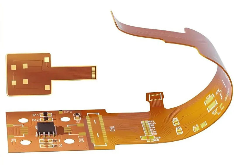
- Rigid zone — standard multilayer construction. Components, connectors, and dense routing live here, and normal rigid-PCB design rules apply.
- Flex zone — only the flex layers continue, with coverlay in place of solder mask. Within this zone, distinguish the active bend area (the section that actually folds or flexes) from flex material that simply routes between rigid sections without bending.
- Transition zone — the boundary where rigid and flex material meet. This is where stress concentrates, and it needs deliberate treatment rather than a straight cut between the two constructions.
These zones should be marked on the mechanical drawing early, in coordination with the enclosure or mechanical design — the available bend area is usually set by the product’s mechanical envelope, not by how the layout happens to route. Defining zones after routing is already underway tends to force rework once the mechanical fit is checked.
What Can Enter Each Zone: Traces, Vias, Pads, and Components
Rather than a blanket rule (“no vias in flex”), what belongs in each zone depends on how much stress that area sees and how often.
| Zone | Traces | Vias | Pads / Components |
|---|---|---|---|
| Rigid zone | Standard rules apply | Standard rules apply | Standard placement |
| Static flex zone | Allowed, routed to minimize stress | Generally avoided; if unavoidable, confirm construction with the fabricator | Avoided where possible; reinforced with local stiffener if placement is unavoidable |
| Dynamic flex zone | Perpendicular to the bend line, rounded transitions, minimal layer count | Avoided | Avoided |
| Transition zone | Staggered layer end points, not a single flush cut | Avoided at the boundary line itself | Avoided directly at the boundary |
The reasoning behind these conditions matters more than the table itself:
- Traces in flex sections are typically routed perpendicular to the bend line rather than parallel to it, since a trace running parallel to a fold sees repeated tension across its full width. Rounded corners are preferred over 90-degree turns for the same reason — a sharp corner is a stress concentration point.
- Vias in flex material represent a discontinuity in the copper at exactly the kind of location that’s already under mechanical stress, which is why they’re avoided in active bend areas rather than treated as a routine routing choice.
- Components and connectors placed in flex zones concentrate stress at the solder joint and at any adhesive-backed stiffener under the part. Where board space doesn’t allow moving a component into a rigid section, some designs use a reinforced “rigid island” within the flex material — a local stiffener under that specific component — rather than leaving it unsupported on bare flex.
None of this should be read as an absolute prohibition. It’s a judgment call based on how much flexing that specific zone will actually see, and it’s worth confirming with the fabricator once the layout is close to final, since process capability varies.
Coverlay, Local Stiffening, and Managing Transition Stress
Coverlay replaces solder mask over the flex layers and is the main protection for the flex copper. Openings in the coverlay need clearance around solder pads, and should not be cut right at a fold line — a coverlay opening at the point of maximum bend removes protection exactly where the copper needs it most.
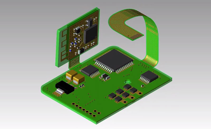
Local stiffeners — typically FR4, polyimide, or stainless steel bonded to the back of the flex material — serve two purposes: giving components in flex sections something rigid to solder onto, and spreading load across a wider area at connectors or transitions instead of letting it concentrate at one edge. Material and thickness choice depends on how much rigidity that specific location needs and what the fabricator’s bonding process supports — this is worth a direct conversation with the fab rather than a generic default.
Transition stress is one of the more common sources of field failures in rigid-flex boards, and it usually comes from a few recurring causes: all layers ending at the same line instead of staggered end points, a sharp rigid-to-flex edge instead of a chamfered or radiused one, and a bend radius that’s tighter than the construction supports right at the boundary. The fix in most cases is geometry — staggering the layer transitions and controlling the radius at the fold — rather than simply adding more material thickness at the joint.
Communicating Bend Requirements in Mechanical Drawings and Fab Notes
The layout alone doesn’t tell a fabricator how the board is meant to be built. The mechanical drawing needs explicit callouts:
- Bend direction (which side of the flex faces outward after folding)
- Final folded position and angle
- Minimum bend radius for each flex section
- Keep-out areas near bend lines where tooling or handling during assembly could stress the board
Fab notes should separately specify coverlay opening tolerances, stiffener placement and thickness, and any via or component keep-out distance from the bend line. Bend radius itself depends on copper weight, layer count, dielectric thickness, and how many flex cycles the section needs to survive — it’s a calculation tied to the specific construction rather than one number that applies across designs, which is why it’s worth working through as its own step once the construction is set.
Leaving these details to be inferred from the Gerber files is a common reason rigid-flex designs get sent back for clarification during fab review — the electrical layout can be complete while the mechanical build intent is still ambiguous.
DFM Confirmation Before Design Freeze
Before locking the design, confirm the following with the fabricator rather than assuming they’ll be caught downstream:
- Bend zones and transition geometry match what the fab’s process can actually build
- Copper type and flex construction match the required flex cycle life for dynamic sections
- Coverlay opening tolerances and stiffener placement are shown on the fab drawings, not just implied by the layout
- Mechanical drawing bend callouts match how the board is actually folded and installed during assembly
- Any components or connectors placed near a transition zone have been reviewed for stress risk at that specific location
Working through bend type, zone definitions, and transition details before layout freeze is what keeps rigid-flex designs from needing structural rework after DFM review. Stackup construction, material selection, and bend radius calculation each follow as their own decisions once these zones and requirements are defined. Understanding how those requirements move through the rigid-flex PCB manufacturing process also makes fabricator feedback easier to evaluate. For formal flex and rigid-flex design requirements, consult the current revision of IPC-2223.