
Rigid-flex PCB fabrication brings a flexible circuit and a rigid multilayer structure together in one panel. The sequence matters because the flex section must survive lamination, drilling, plating, finishing, and panel handling without being bonded, contaminated, or damaged in areas that must remain flexible.
Process overview: stackup and material confirmation → flex-circuit fabrication → rigid-layer preparation → combined lay-up and lamination → drilling and metallization → outer-layer finishing → flex-area opening and profiling → electrical and physical inspection.
Table of contents
- The Process Starts with Separate Flex and Rigid Builds
- Lay-Up and Lamination Define the Rigid-Flex Structure
- Drilling and Metallization Connect the Combined Stack
- Outer-Layer Finishing Is Familiar, but the Boundary Still Matters
- Opening the Flex Areas and Forming the Final Outline
- Final Inspection Must Verify More Than Continuity
The Process Starts with Separate Flex and Rigid Builds
Production begins with a review of the released stackup, fabrication drawing, material callouts, panel data, and layer files. The manufacturer checks that the flex and rigid portions can be combined in the stated sequence and that the selected bonding materials, coverlay openings, copper constructions, and finished thickness targets are compatible with the planned process.
This review is followed by material preparation. Copper-clad polyimide, coverlay, bonding films or no-flow prepreg, rigid cores, and prepreg are cut and prepared for the production panel. Registration features, tooling holes, and panel support are planned at the same stage because the flexible sections will need controlled handling later in the build.
Flex-circuit imaging, etching, and coverlay
The flexible circuit is formed on copper-clad polyimide. The copper pattern is imaged and etched, then checked before it is buried inside the combined construction. The exact inspection method depends on the factory and the design, but the purpose is the same: verify trace geometry and registration while the flex layers are still accessible.
Coverlay is aligned and laminated over the flex circuitry, leaving openings where pads or other exposed copper must remain accessible. Coverlay registration is particularly important near fine-pitch pads and transition areas. An opening that shifts can expose copper unintentionally or cover part of a connection area.
Rigid inner-layer preparation
The rigid inner layers are processed using the familiar imaging and etching sequence used for multilayer rigid PCBs. At this point, the two builds are still separate: the flex circuit has its copper pattern and coverlay, while the rigid layers are prepared to surround or connect to it during lay-up.
Lay-Up and Lamination Define the Rigid-Flex Structure
This is the stage that most clearly separates rigid-flex fabrication from conventional multilayer PCB production. The finished flex circuit, rigid inner layers, and bonding materials must be positioned so that the rigid areas bond completely while the intended flex areas remain free to bend.
Protecting the future flex area
During lay-up, the manufacturer creates a controlled boundary between the rigid and flexible regions. Depending on the construction, this can involve no-flow bonding material, release films, temporary fillers, routed openings in rigid materials, or a combination of these methods. Their purpose is not merely to hold the stack together. They must also prevent resin from flowing into the flex zone and avoid leaving a hard edge or bonded area where movement is required.
The transition region deserves more attention than the center of either the rigid or flex section. Material edges, adhesive flow, coverlay termination, and registration all meet in a narrow area. A well-formed panel can still develop problems later if resin enters the bend zone, if the rigid opening is misregistered, or if the transition edge is damaged during subsequent processing.
Pressing the combined panel
The laid-up panel is laminated under a controlled heat-and-pressure cycle. The cycle must bond the rigid substack and the flex circuit without shifting the layers or compromising the flexible region. Press parameters are selected for the materials and construction being built; they are not universal rigid-flex settings.
Some designs require sequential lamination because of buried or blind interconnects, multiple flex depths, or other structural requirements. That does not make sequential lamination a standard step for every rigid-flex board. It adds process stages only when the stackup requires them, and each additional cycle increases the importance of registration, thickness control, and intermediate inspection.
Drilling and Metallization Connect the Combined Stack
After lamination, the panel is drilled for through-holes and any other holes formed at this stage. The drill passes through a mixed construction that may include rigid laminate, bonding material, and polyimide. Drill parameters, entry and backup materials, and hole-cleaning methods therefore need to match the actual stack rather than an all-FR-4 assumption.
Hole-wall residue is removed before metallization. Chemical desmear, plasma treatment, or another preparation route may be used according to the resin system, polyimide exposure, hole geometry, and plating process. Plasma is useful in some rigid-flex builds, but it should not be described as a mandatory step for every construction.
Electroless copper establishes conductivity on the prepared hole walls, and electrolytic plating builds the required copper thickness. Outer-layer imaging and etching then form the external circuitry. These operations resemble conventional multilayer PCB processing, although registration and panel support still need to account for the embedded flex sections.
Outer-Layer Finishing Is Familiar, but the Boundary Still Matters
Solder mask is applied to the rigid outer surfaces, while coverlay protects the flexible circuitry. The interface between the two should leave the intended copper covered without creating an unwanted stiff or exposed region at the transition.
The selected surface finish is applied to exposed pads and contact areas. ENIG, immersion silver, HASL, and other finishes may be used when compatible with the design and assembly requirements. Surface finish selection is not unique to rigid-flex fabrication, so it should be treated as a product and assembly decision rather than a defining rigid-flex process step.
Opening the Flex Areas and Forming the Final Outline
Once the plated and finished structure is complete, the flexible sections must be exposed. The manufacturer removes the rigid material, temporary support, or release construction that covered the flex area during earlier processing. The exact operation varies with the panel design and may involve controlled-depth routing, laser processing, punching, or previously formed openings.
This step has two competing requirements: remove the unwanted rigid material cleanly, but do not nick, score, overheat, or delaminate the flex circuit below it. Edge quality is especially important where the exposed flex exits the rigid section. Damage introduced there can remain hidden until the board is folded or moved in the product.
The final board outline is then routed, laser-cut, punched, or produced with a combination of methods appropriate to the rigid and flexible edges. Boards may be supplied flat or formed to a specified shape, depending on the released drawing and the downstream assembly process. Static and dynamic bend applications place different demands on the finished flex section, but bend-life qualification belongs to material, design, and reliability planning rather than to this fabrication sequence alone.
Final Inspection Must Verify More Than Continuity
Electrical testing checks continuity and isolation against the netlist. The method may be flying probe or fixture-based, depending on panel design, volume, and test strategy.
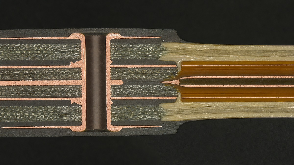
Physical inspection then addresses features that electrical test cannot evaluate:
- coverlay and solder-mask registration;
- flex-area cleanliness and freedom from unwanted resin;
- transition-edge quality and signs of lifting or delamination;
- finished dimensions and rigid-to-flex alignment;
- hole-wall plating, layer registration, and lamination quality through microsection coupons where required.
Microsectioning is destructive, so it is performed on representative coupons or samples rather than on every finished board. It provides a cross-sectional view of plated holes, internal registration, bonding interfaces, and other features that cannot be confirmed from the surface.
In practical rigid-flex PCB fabrication, a completed board is the result of two controlled builds and one carefully managed joining operation. Imaging, drilling, plating, solder mask, and surface finish are established PCB processes; the distinguishing work lies in preserving the flexible region while those processes are carried out and verifying that the rigid-to-flex transition remains intact at the end.
Qualification and performance requirements for flexible and rigid-flex printed boards are covered by IPC-6013. The applicable revision and acceptance class should be agreed before fabrication begins.