
An automatic blood pressure monitor may appear relatively simple, but its electronics bring together several functional areas: pressure sensing, analog signal processing, digital computation, pump and valve control, power management, and the user interface.
In a typical automatic oscillometric blood pressure monitor, the MCU controls cuff pressure through the pump and valve while the pressure sensor continuously tracks pressure changes inside the cuff. After signal conditioning and digitization, the sensor output returns to the MCU for measurement processing and further control of the pneumatic system.
The measurement cycle is therefore not a one-way signal path. It is a closed-loop system in which pressure acquisition and pneumatic control work together.
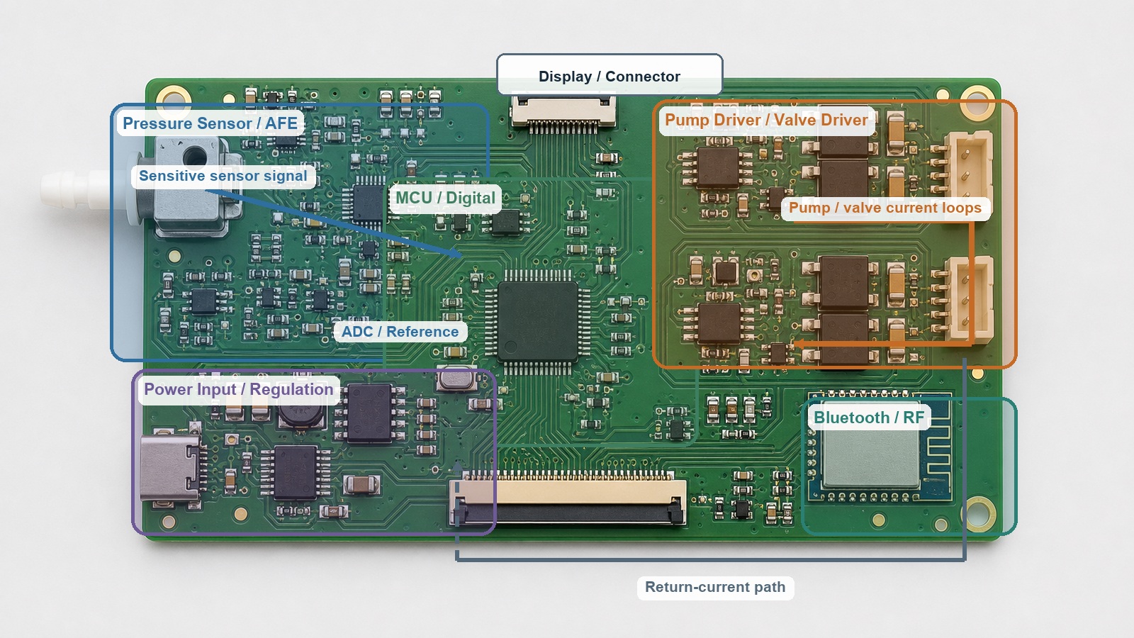
From an electronics perspective, a blood pressure monitor PCBA generally has to handle two very different circuit types: a noise-sensitive pressure measurement chain and pump and valve driver circuits that carry much higher switching currents.
This article uses a simplified blood pressure monitor circuit architecture to explain how the pressure sensor, analog front end (AFE), analog-to-digital converter (ADC), microcontroller (MCU), pump, valve, and power-management circuitry work together. It also examines what this architecture means for PCB implementation and PCBA manufacturing.
Table of contents
- Blood Pressure Monitor Circuit Diagram at a Glance
- From Cuff Pressure to a Digital Signal
- How the Pump and Valve Control Cuff Pressure
- MCU, Display, Memory, and Connectivity
- Power Management Connects Two Very Different Electrical Loads
- Why a Blood Pressure Monitor PCB Is a Mixed-Signal System
- What This Architecture Means for PCBA Manufacturing
- From Electronic Architecture to a Manufacturable PCBA
Blood Pressure Monitor Circuit Diagram at a Glance
Different digital blood pressure monitors use different components and circuit implementations, but their basic functions can usually be organized into three interconnected paths.
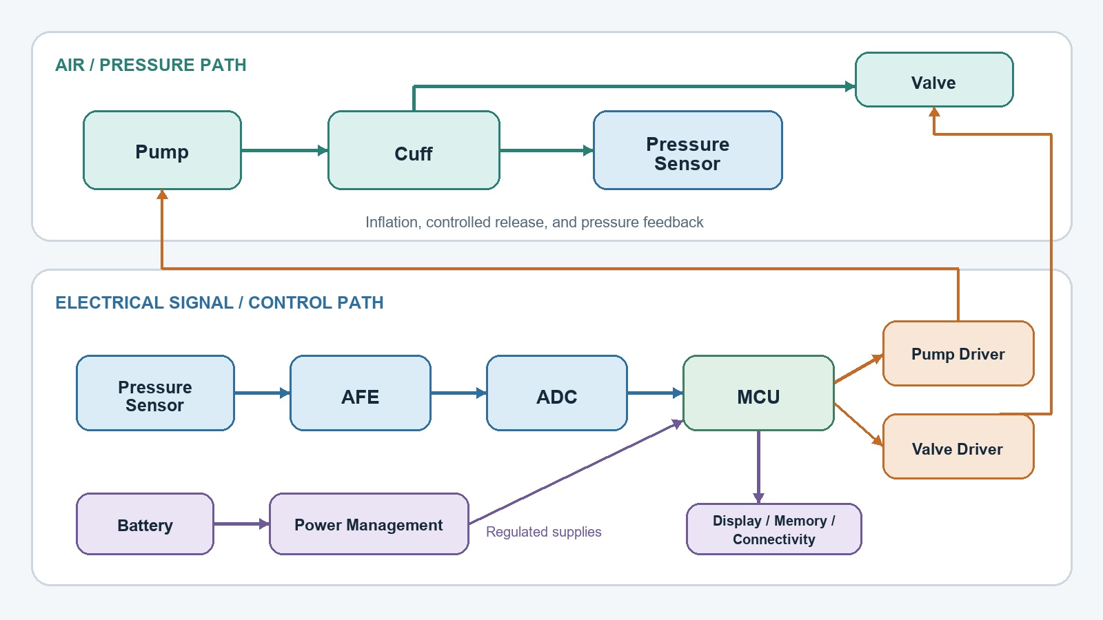
Pneumatic path
Pump / Valve <-> Cuff -> Pressure Sensor
The pump inflates the cuff, the valve regulates or releases air as required by the measurement sequence, and the pressure sensor continuously detects pressure changes in the pneumatic path.
Measurement signal path
Pressure Sensor -> Signal Conditioning / AFE -> ADC -> MCU
This path converts cuff pressure changes, including the small pulse-related oscillations within the pressure waveform, into data the MCU can process.
Control path
MCU -> Pump Driver -> Pump
MCU -> Valve Driver -> Valve
In addition to pressure measurement and pneumatic control, the MCU commonly connects to the display, user interface, memory, and connectivity modules. A battery or other power input supplies the pressure sensor, analog front end, MCU, display, and driver circuits through the power-management circuitry.
At the system level, the main functional areas can be summarized as follows:
| Functional area | Typical elements | Primary role | PCB / PCBA focus |
|---|---|---|---|
| Pressure sensing | Pressure sensor, AFE, ADC | Acquire cuff pressure and oscillation signals | Low-noise routing, stable power, reference stability |
| Digital processing | MCU, memory | Process data and control the system | Power integrity, interface reliability |
| Pneumatic control | Pump, valve, drivers | Inflate, regulate pressure, and deflate | Switching current, driver circuitry, current paths |
| User interface | Display, buttons, buzzer | Present results and accept user input | Connectors, flex cables, mechanical interfaces |
| Power management | Battery input, regulators | Supply each functional area | Noise control, transient response, current distribution |
These functional areas do not operate independently. The MCU reads pressure data while controlling the pump and valve so that cuff pressure follows the required measurement sequence.
From Cuff Pressure to a Digital Signal
An automatic blood pressure monitor must first convert mechanical pressure in the cuff into data that the electronic system can recognize and process.
This conversion usually involves a pressure sensor, signal-conditioning circuitry, an ADC, and an MCU, although these functions do not necessarily correspond to separate integrated circuits.
Pressure Sensor
The pressure sensor is the critical interface between the pneumatic path and the electronic system.
The cuff connects to the pressure sensor through tubing, a pneumatic channel, or a manifold. As cuff pressure changes, the sensor produces a corresponding electrical output.
The implementation varies with the sensor type. Some sensors provide an analog output and require external amplification, filtering, and analog-to-digital conversion. Others integrate part of the signal conditioning and may even provide a digital output directly.
For this reason, the sequence below is best understood as a functional signal chain rather than a fixed count of separate devices:
Pressure Sensor -> AFE -> ADC
In oscillometric blood pressure measurement, the pressure-sensor output represents the overall cuff pressure profile while also carrying much smaller pressure oscillations caused by arterial pulsation. The analog front end and subsequent digital processing must preserve and extract useful information from this combined waveform.
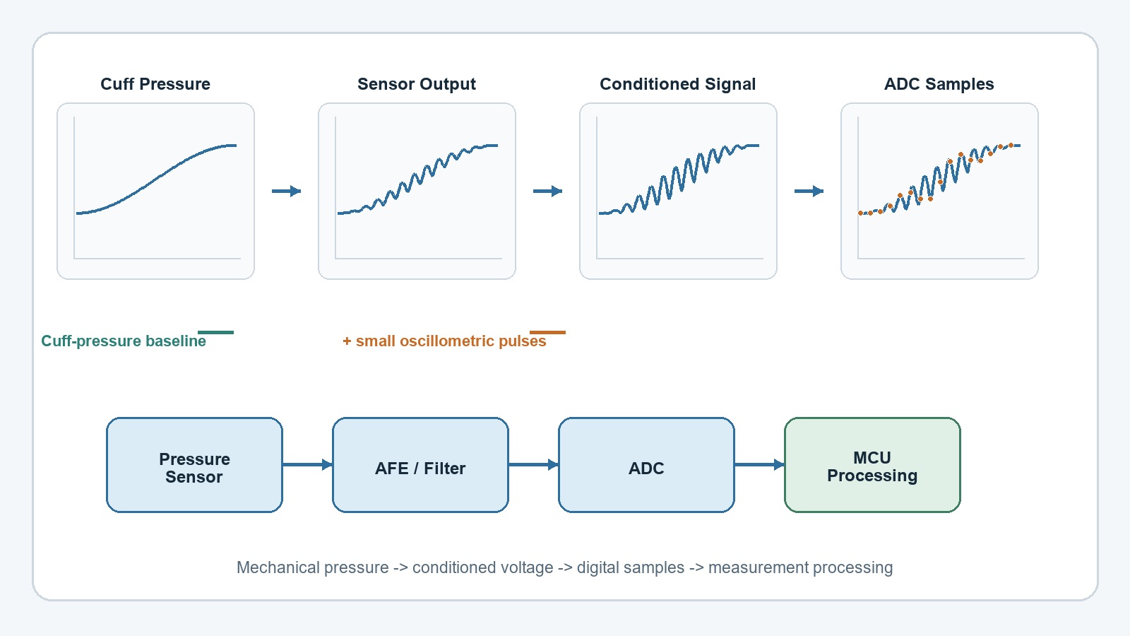
Because the useful oscillometric component is relatively small, the circuitry around the pressure sensor is generally more susceptible than ordinary digital I/O to supply noise, return-path effects, and nearby switching circuits.
Signal Conditioning and Filtering
The raw pressure-sensor signal normally requires conditioning before it enters the digital system.
Depending on the design, signal conditioning may include:
- amplification and gain control;
- filtering;
- biasing;
- analog front-end circuitry; and
- ADC input conditioning.
Together, these functions keep the ADC input within an appropriate amplitude and bandwidth while reducing the influence of irrelevant noise on the measurement data.
In a blood pressure monitor, this sensitive analog circuitry does not operate in an electrically quiet PCB environment.
The same PCBA usually includes pump and valve drivers. Starting and stopping the pump motor and switching the valve produce significant current changes. These disturbances can reach the pressure measurement chain through the power rails, ground-return paths, or electromagnetic coupling.
Signal-conditioning performance therefore depends not only on the components shown in the schematic but also on PCB layout and power distribution.
ADC and Reference
The ADC sits between the analog measurement chain and the digital processing system.
It converts the conditioned pressure signal into digital data for further processing by the MCU.
In a real system, ADC performance is not determined by nominal resolution alone. Signal-acquisition quality also depends on:
- input signal quality;
- reference stability;
- supply noise;
- grounding and return paths; and
- PCB coupling.
The areas around the ADC, voltage reference, and analog front end therefore require particular attention on a blood pressure monitor PCB.
How the Pump and Valve Control Cuff Pressure
If the pressure sensor detects what is happening inside the cuff, the pump and valve actively change the cuff pressure.
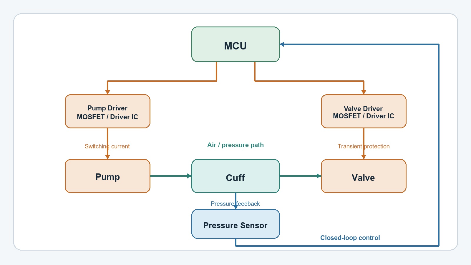
An automatic blood pressure monitor must inflate the cuff, regulate pressure, and release pressure according to the measurement sequence. The MCU therefore controls these electromechanical loads through dedicated driver stages.
Air Pump
A miniature air pump supplies air to the cuff.
The MCU normally does not source the pump motor current directly. Instead, it controls the pump through a MOSFET, transistor, motor-driver IC, or another power stage.
A typical control relationship is:
MCU -> Pump Driver -> Pump
Compared with the pressure sensor and analog front end, the pump driver usually carries much more current. For the PCB, it is therefore not only a logic-control circuit but also a power path that requires attention to the supply, copper current path, decoupling, and switching-current loop.
Valve Control
The valve controls the release of air from the cuff.
Different blood pressure monitors may use different valves and pneumatic architectures, so there is no single universal driver circuit. Functionally, however, most systems include a relationship similar to:
MCU -> Valve Driver -> Valve
If the selected load is significantly inductive, the driver circuit must include suitable transient suppression or protection for that specific device.
More importantly, the pump and valve do not operate independently of the measurement chain. Their control is always related to the data returned by the pressure sensor, so pneumatic control and pressure measurement form a complete feedback loop.
MCU, Display, Memory, and Connectivity
The MCU usually serves as the central controller for the electronic system.
Depending on the product design, it may be responsible for:
- pressure-data acquisition;
- pump and valve coordination;
- measurement-related digital processing;
- display and button control;
- data storage and communications; and
- system-status and fault monitoring.
In an automatic oscillometric blood pressure monitor, the MCU also processes the oscillation information in the pressure waveform and generates measurement results using the algorithm implemented by the device developer.
The distinction here is important: the blood-pressure calculation algorithm and final measurement performance belong to the design and validation scope of the medical device itself. The role of PCBA manufacturing is to reproduce the approved hardware design consistently, not to redefine the customer’s measurement algorithm.
For user interaction, the device may also include an LCD, buttons, LEDs, a buzzer, or other interface elements. Although these components may not belong to the most sensitive measurement area, they affect connector arrangement, flex-cable interfaces, PCB dimensions, component placement, and mechanical assembly.
Modern blood pressure monitors may also include nonvolatile memory, USB, Bluetooth, Wi-Fi, or other wireless connectivity. As these functions are added, the relationships among digital, RF, power-supply, and interface circuits on the PCBA become more complex.
Two devices can therefore both be blood pressure monitors while having very different PCB architectures and assembly requirements.
Power Management Connects Two Very Different Electrical Loads
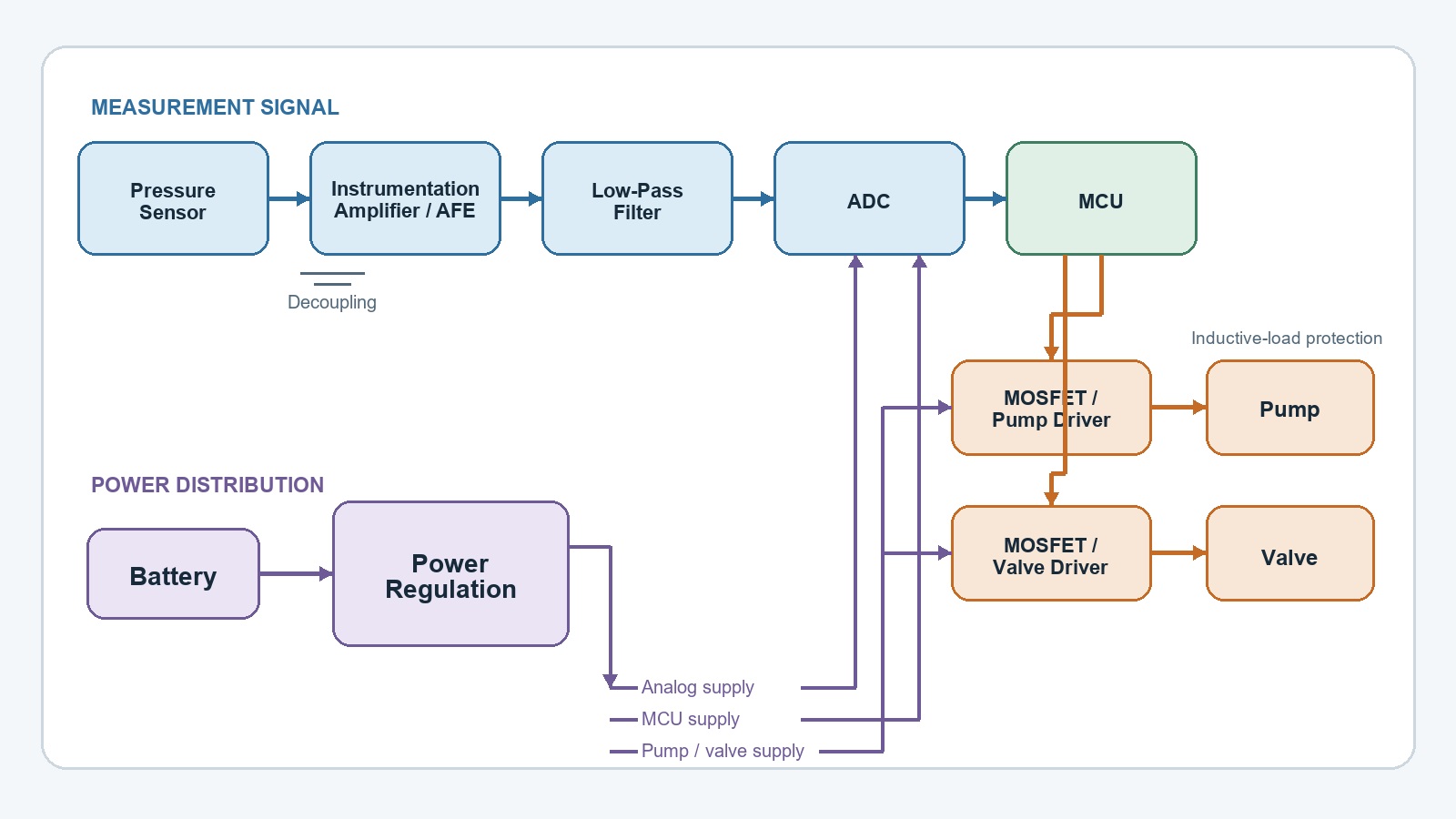
A blood pressure monitor has a characteristic power architecture: the same system must support both sensitive measurement circuitry and electromechanical loads.
The pressure sensor, AFE, ADC, voltage reference, and MCU depend on stable, low-noise power. The pump and valve, by contrast, generally draw higher transient current and can create substantial supply disturbances when they start, stop, or switch.
This places two very different electrical environments on the same PCB:
Sensitive low-level measurement
and
Higher-current switching loads
If their power paths and return-current paths are not managed appropriately, pump or valve operation can disturb the measurement area through supply variation or ground coupling.
A design may therefore use separate supply rails, local decoupling, filtering, or deliberate current-path planning to reduce interaction between the two areas. The appropriate approach depends on the power budget, PCB size, battery architecture, and measurement-performance requirements; no single arrangement suits every blood pressure monitor.
Why a Blood Pressure Monitor PCB Is a Mixed-Signal System
From a PCB engineering perspective, an automatic blood pressure monitor is a typical mixed-signal system.
The same PCB may contain three circuit groups with very different characteristics:
- Sensitive analog circuits: pressure sensor, AFE, ADC, and voltage reference;
- Digital circuits: MCU, memory, and digital interfaces; and
- Power and switching circuits: pump and valve drivers.
If the device includes Bluetooth or another wireless interface, RF circuitry may add a fourth functional area.
A PCB layout cannot therefore be treated as a simple exercise in connecting every schematic net.
The design also has to consider where the pressure sensor and analog front end should be placed, whether sensitive analog routes are close to high-di/dt switching paths, where pump and valve current enters and returns, and whether decoupling, connector placement, or power distribution changes the actual return-current paths.
The goal is not to divide the analog, digital, and power areas into three mechanically isolated zones.
For a mixed-signal PCB, the more useful questions are: Where are the high-current switching loops? Where are the sensitive signals? Do they share an unsuitable power or return path?
This is why blood pressure monitor PCB layout often requires a coordinated tradeoff among signal integrity, power control, PCB size, and mechanical constraints.
What This Architecture Means for PCBA Manufacturing
When an established electronic design enters production, its circuit architecture becomes a set of practical requirements for component placement, soldering, inspection, and functional testing.
For a PCBA manufacturer, understanding these functional areas is not about redesigning the customer’s blood pressure monitor. It is about identifying manufacturing risks accurately and establishing appropriate processes and inspection plans for the actual components and project requirements.
Component Placement and Assembly
A blood pressure monitor PCBA may combine precision analog components, an MCU, MOSFETs, driver ICs, a pressure sensor, connectors, and passive components in several sizes.
These components differ in package style, pad geometry, and thermal behavior. For example, a package with an exposed pad may need a different solder-paste design and exhibit different reflow behavior from a conventional leaded package. Large connectors and small passive components also impose different placement and soldering requirements. These considerations are addressed during solder paste printing and subsequent SMT assembly.
Reviewing the PCB data, BOM, component packages, and assembly drawing during NPI can help identify common issues early, including:
- package-related assembly risks;
- polarity and orientation;
- exposed-pad soldering;
- connector-related solder joints; and
- BOM availability and approved-substitution requirements.
The manufacturing approach should ultimately follow the actual design rather than applying one fixed process simply because the product is a medical device.
Inspection Should Follow the Actual Package
The inspection plan should likewise be based on the actual package structures and project requirements.
For visible SMT solder joints, AOI can check for missing components, polarity errors, placement offsets, and visible solder defects that can be recognized optically.
If the design uses BGA, LGA, QFN, or another package with hidden solder joints, the package structure, assembly risk, and customer inspection requirements should determine whether X-ray inspection is appropriate and what level of inspection is needed. The same package-specific logic is central to reliable BGA assembly.
The fact that a product is a blood pressure monitor does not, by itself, define a fixed inspection combination. A more appropriate relationship is:
Component Package + Assembly Risk + Project Requirement -> Inspection Strategy
Functional Verification at PCBA Level
Board-level functional testing must be based on the firmware, test fixture, test procedure, and acceptance criteria supplied by the customer.
Depending on the design, testing may cover:
- power-up behavior and current consumption;
- firmware programming;
- pump and valve control outputs;
- sensor-interface response;
- ADC-related response; and
- display or communication interfaces.
If the project includes a suitable pressure fixture or test method, the response of part of the pressure-signal path may also be verified. This is one application within the broader range of PCB assembly testing methods.
However, it is essential to distinguish between:
PCBA functional testing
and
Finished blood pressure monitor calibration and performance validation
The first confirms that the board-level hardware operates according to defined requirements. The second addresses the complete device, including measurement accuracy, the algorithm, the pneumatic system, the mechanical structure, and product-level validation.
PCBA functional testing therefore cannot replace final calibration, performance validation, or regulatory-compliance confirmation for the finished blood pressure monitor.
From Electronic Architecture to a Manufacturable PCBA
A blood pressure monitor circuit diagram does more than show how the pressure sensor, pump, valve, and MCU are connected.
From a PCB and manufacturing perspective, its greater value is that it reveals why this product contains several very different engineering requirements:
Precision Pressure Sensing + Digital Processing + Pump and Valve Control + Power Management
The pressure sensor and analog front end need a stable signal environment, while the pump and valve introduce much larger current variations. The MCU, display, memory, and connectivity functions add further interaction among the functional areas.
When the device design moves into PCB and PCBA production, the component packages, sensitive-signal areas, power paths, soldering process, inspection coverage, and board-level functional testing must all be defined for the actual product design.
For medical-device developers, the manufacturing objective is not to alter the approved electronic architecture. It is to turn approved design data into consistent, traceable PCB assemblies within an appropriate ISO 13485 medical PCB assembly and manufacturing framework.
SugaMed provides blood pressure monitor PCB assembly based on customer-supplied PCB data, BOMs, firmware, inspection criteria, and test requirements, including PCB/PCBA manufacturing, assembly, inspection, and applicable board-level functional testing.