
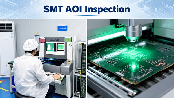
Automated optical inspection, or AOI, is one of the most common inspection steps in modern SMT assembly. After reflow, an AOI system can check for missing or misaligned components, polarity errors, tombstoning, visible solder bridges, and other defects that can be identified optically.
That makes AOI an important part of PCB assembly quality control. But an AOI pass does not mean a PCBA has completed all necessary quality verification.
AOI is still an optical inspection method. It is highly effective for visible assembly features, but it cannot see through a BGA package, verify firmware operation, or confirm that a board performs correctly when powered.
To understand where AOI inspection adds value, it helps to look at three questions: how it works, what it can detect, and where other inspection or testing methods are still required.
What Is AOI Inspection in SMT Assembly?
AOI stands for Automated Optical Inspection.
In SMT assembly, AOI systems use cameras, controlled lighting, and image-processing or measurement algorithms to inspect components and visible soldering features on an assembled PCB.
The system compares what it sees or measures against an inspection program built from PCB and component data, component libraries, reference information, and defined acceptance criteria.
AOI is especially useful when a board contains hundreds or thousands of repetitive visual features.
Relying entirely on manual visual inspection at that scale introduces obvious limitations in speed, repeatability, and operator fatigue. AOI can inspect the same locations using consistent programmed criteria and flag suspicious areas for further review.
Its basic limitation follows from the same principle: AOI can only evaluate features that the optical system can see and the inspection program can recognize.
How Does AOI Inspection Work?
Before an AOI program is released to production, an inspection program must first be created for the PCB assembly.
Depending on the AOI platform, programming may use PCB design data, component information, libraries, reference boards, or combinations of these inputs. Inspection criteria are then established for characteristics such as component position, orientation, polarity, dimensions, markings, and visible solder features.
When a PCB enters the AOI system, fiducials or other reference features are typically used to align the physical board with the inspection program.
The system then captures images under controlled lighting.
A 2D AOI system primarily evaluates planar image characteristics such as position, shape, area, color, contrast, and visible geometry. A 3D AOI system can add height and surface-profile information.
The software compares the measured features with the programmed criteria. If something falls outside the accepted range, such as a shifted component, reversed polarity, or a suspected solder bridge, the location is flagged for review.
An AOI alarm does not automatically mean the board has a real defect.
Reflections, shadows, component appearance variation, board warpage, and inspection thresholds can all contribute to false calls. Criteria that are set too loosely can create the opposite problem: an actual defect may escape detection.
For this reason, AOI performance depends on much more than camera resolution or machine specifications. Program quality, lighting, inspection criteria, verification, and defect review all affect the reliability of the inspection process.
Where Does AOI Fit in the SMT Process?
A simplified SMT process may look like this:
Solder Paste Printing -> SPI -> Component Placement -> Reflow Soldering -> AOI -> Additional Inspection or Testing
After solder paste printing, solder paste inspection (SPI) is better suited to checking paste height, area, volume, and positional offset before components cover the pads.
Some production lines also use pre-reflow AOI after component placement to identify missing, shifted, or incorrectly oriented parts before soldering.
Post-reflow AOI is especially common because the components have already been soldered in place. At this stage, the system can inspect final component position as well as visible conditions such as solder bridging, tombstoning, lifted leads, and other accessible solder-joint abnormalities.
Boards containing BGA, LGA, QFN, or other bottom-terminated packages may require X-ray inspection because significant portions of their solder connections are hidden from optical view.
ICT, flying probe testing, or functional testing may then be added depending on the PCB design, test access, product function, and project-specific test plan.
These methods are not simply performing the same inspection several times. Each one addresses different failure modes.
What Defects Can AOI Detect?
AOI works best when a defect creates a clear, repeatable visual feature.
| Inspection Area | Typical Defects AOI Can Detect | Key Limitation |
|---|---|---|
| Component presence | Missing components and some incorrect components | Parts must be distinguishable by package, appearance, or marking |
| Placement | Shift, rotation, skew | Capability depends on optical access and programmed tolerances |
| Orientation | Incorrect orientation | The component must have identifiable orientation features |
| Polarity | Reversed diodes, electrolytic capacitors, and similar parts | Polarity markings must be visible and distinguishable |
| Passive components | Tombstoning, billboarding | Usually produces a clear geometric change |
| Soldering | Visible solder bridges and some excess or insufficient solder conditions | Only accessible solder regions can be evaluated |
| Leads | Lifted or misaligned visible leads | 3D data can improve height and coplanarity evaluation |
The word visible matters.
A resistor can be installed in the correct position and look completely normal while still being electrically damaged. AOI cannot determine its internal electrical condition from appearance alone.
Similarly, if two resistor values use packages and markings that cannot be reliably distinguished optically, AOI cannot turn visual inspection into electrical component verification.
2D vs. 3D AOI: What Is the Difference?
2D AOI evaluates information from planar images.
It is well suited to checking component presence, X-Y position, rotation, polarity, and many visible solder characteristics. However, reflections, shadows, tall components, and complex solder geometry can make some conditions difficult to evaluate from a two-dimensional image alone.
3D AOI inspection adds Z-axis information.
Using structured light or other 3D measurement methods, the system can measure the height and surface profile of components and solder features. This can improve inspection of lifted leads, component tilt, coplanarity, tombstoning, and some visible solder geometries.
| Capability | 2D AOI | 3D AOI |
|---|---|---|
| Missing component | Yes | Yes |
| Position and rotation | Yes | Yes |
| Polarity and orientation | Yes | Yes |
| Height measurement | Limited | Yes |
| Lifted component or lead | More dependent on viewing angle and shadow | Easier to quantify |
| Coplanarity | Limited | Better suited |
| Visible solder profile | Based mainly on 2D visual features | Can include height and surface-profile data |
| Hidden BGA solder joints | No | No |
The last row is important.
3D AOI is not X-ray inspection.
Adding height information improves optical inspection, but the system is still limited by line of sight. If a solder joint is completely hidden underneath a BGA package, a camera cannot see through the package to inspect the connection.
What AOI Cannot Reliably Detect
Visibility is one of AOI’s most important limitations.
BGA solder balls are located underneath the package. LGA, QFN, and other bottom-terminated components can also contain solder regions that cannot be fully viewed from outside the package.
AOI may confirm that a BGA is present and correctly positioned, but it cannot directly inspect the condition of every hidden solder joint.
That is where X-ray inspection or AXI becomes more appropriate.
Hidden joints are not the only limitation.
AOI also cannot directly verify firmware operation, communication interfaces, MCU behavior, or complete circuit functionality. A PCBA can look normal under optical inspection and still contain an open circuit, incorrect component value, damaged IC, or firmware-related problem.
This is why:
AOI PASS does not mean the PCBA functions correctly.
Some defects also fall into a gray area. AOI may flag an obviously abnormal visible solder joint, but a joint that looks normal externally can still contain conditions that optical inspection cannot evaluate.
AOI provides valuable visual evidence. It should not be treated as proof that every possible failure mode has been eliminated.
AOI vs. SPI vs. X-Ray vs. Electrical and Functional Testing
Instead of asking which inspection method is “best,” a more useful question is:
What failure mode are we trying to detect, and which method can actually observe it?
| Method | Primary Inspection or Test Target | Typical Stage | Main Limitation |
|---|---|---|---|
| SPI | Solder paste height, area, volume, and offset | After printing, before placement | Does not inspect final solder joints or product function |
| AOI | Visible component, placement, and soldering defects | After placement or reflow | Cannot fully inspect hidden joints or electrical function |
| X-Ray / AXI | Hidden solder joints and internal structures | After reflow | Does not prove complete electrical or functional performance |
| ICT / Flying Probe | Opens, shorts, selected component values, and accessible networks | After assembly | Coverage depends on test access and circuit design |
| Functional Test | Defined powered functions | After assembly | Only verifies functions included in the test specification |
A robust PCBA inspection strategy often combines several of these methods.
SPI can identify solder paste variation before placement and reflow. AOI checks visible assembly conditions after placement or soldering. X-ray provides visibility into hidden solder joints. ICT, flying probe, or functional testing then addresses electrical and functional questions that optical inspection cannot answer.
Each method solves a different part of the quality problem.
Why a Good AOI Machine Is Not Enough
Installing a high-performance AOI machine does not automatically create a reliable inspection process.
The first requirement is a correct inspection program.
If the PCB revision changes while production continues using an outdated AOI program, the inspection criteria may no longer match the actual product. Similar problems can occur when the component library does not match the approved BOM or when polarity, position, and solder criteria are poorly defined.
Lighting and optical access also matter.
Highly reflective solder, unusual component surfaces, shadows from tall components, and PCB warpage can change what the camera sees.
Threshold settings create another trade-off.
If inspection criteria are too tight, the system may generate large numbers of false calls. Operators then spend time reviewing assemblies that are actually acceptable.
If the criteria are too loose, real defects may escape detection.
For that reason, effective AOI process control involves more than maintaining the machine. It also requires control of inspection programs, product revisions, criteria, defect classification, verification, and program changes.
IPC-9716 specifically addresses AOI process control for printed board assemblies, reinforcing an important point: evaluating an AOI process requires more than asking whether a factory owns an AOI machine.
AOI Data Can Also Improve the Manufacturing Process
AOI has value beyond separating suspected defective boards from acceptable ones.
When the same solder bridge, placement shift, or tombstoning pattern appears repeatedly, AOI defect data can provide feedback to the manufacturing process.
For example, detecting tombstoning does not explain why it happened.
The engineering team may still need to examine solder paste deposition, pad geometry, placement conditions, component termination characteristics, and the reflow profile.
Used this way, AOI becomes more than an inspection gate. It becomes a source of data for process improvement.
Why AOI Matters in Medical PCB Assembly
AOI is not a medical-specific inspection technology.
A medical PCBA uses the same optical inspection principles as other PCB assemblies, and a BGA solder joint does not become visible simply because the board is used in a medical device.
The difference is often in how AOI is incorporated into the manufacturing and quality-control plan.
For projects requiring stronger documentation and traceability, inspection control may include links between the PCB or PCBA revision, AOI program version, production lot or serial number, defect records, rework status, and reinspection results.
If a problem is discovered later in manufacturing or testing, those records can help trace the issue back to the corresponding production and inspection information.
Inspection coverage should also reflect the actual PCB design.
A board dominated by exposed SMT joints presents a different inspection challenge from one containing multiple BGAs, QFNs, or LGAs. The medical application alone does not determine which inspection method is appropriate.
At SugaMed, prototype SMT assemblies receive 100% post-reflow AOI, while BGA solder joints receive 100% X-ray inspection. X-ray coverage for QFN, LGA, and other bottom-terminated packages is determined according to package characteristics, assembly risk, and project requirements.
The purpose is not simply to apply more inspection equipment to medical electronics. It is to match each inspection method to the failure modes it is capable of detecting.
AOI Works Best as Part of a Complete PCBA Quality-Control Loop
AOI is most useful when viewed as one part of the overall SMT quality-control process.
After solder paste printing, SPI can detect paste-deposition variation before components are placed.
After placement and reflow, AOI examines visible component and soldering conditions.
Hidden solder joints can then be inspected using X-ray or AXI where appropriate.
If the project also requires verification of electrical connectivity or board-level functions, electrical or functional testing can be added according to the test plan.
This does not mean every PCB should automatically pass through every inspection system.
A more practical approach is to identify the likely failure modes of the design and then select inspection and testing methods that provide appropriate coverage.
For purchasing, NPI, and quality teams evaluating a PCB assembly supplier, this also leads to a more useful question than simply asking:
“Do you have AOI?”
A better question is:
“How is AOI used in your SMT process, what defects does it cover, and what inspection or testing methods are used for the areas AOI cannot verify?”
The answer provides much more insight into how the supplier actually controls PCB assembly quality.
Conclusion
AOI inspection is an effective tool for SMT assembly because it can rapidly and consistently evaluate large numbers of visible component-placement and soldering features.
Its limitations are equally important.
AOI can only evaluate features that the optical system can see and the inspection program can reliably identify. Hidden solder joints, electrical conditions, firmware operation, and complete product functionality require other inspection or testing methods.
For medical PCBA projects, the more useful question is not whether an AOI machine is present. It is how AOI, SPI, X-ray, electrical testing, and functional testing are combined according to the PCB design and project risk, and how those inspection results are controlled and traced.
If your medical electronics project is moving into prototype, NPI, or production, SugaMed can review the PCB layout, component packages, BOM, and test requirements to define an appropriate PCBA inspection and testing approach, including AOI, X-ray, and subsequent electrical or functional testing where required.