
Stack-up decisions made before routing begins determine whether your board passes EMI pre-compliance, whether controlled-impedance traces can be manufactured within tolerance, and what the board costs to fabricate. Change the dielectric thickness after routing, and every impedance‑controlled net needs adjustment. Change the layer count, and the layout starts over. This guide covers how to make those decisions in the right order.
Table of Contents
- How Many Layers Your Design Actually Needs
- Layer Ordering for Signal Integrity and EMI Control
- Planning Controlled Impedance Into the Stack‑Up
- Core and Prepreg: What Controls the Final Pressed Thickness
- Copper Weight Decisions by Layer
- Working with Your Fabricator: Standard Versus Custom Stack‑Ups
- Decision Sequence Before You Route
How Many Layers Your Design Actually Needs
Layer count is not determined by component count alone. The decision follows from routing density, reference‑plane requirements, the number of independent power rails, and the high‑speed interface count.
A 4‑layer board — Signal / Ground / Power / Signal — works for designs with moderate routing density, one high‑speed interface, and two to three power rails, provided the ground plane is continuous and critical signals do not reference the power plane.
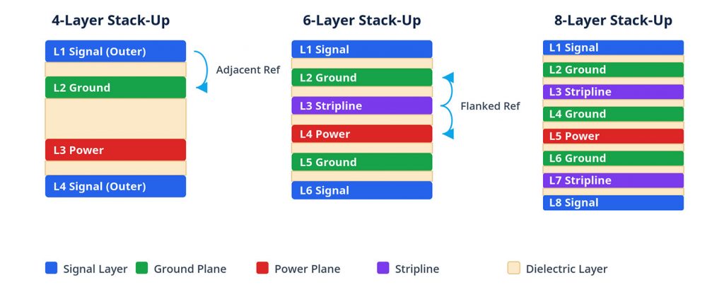
A 6‑layer board becomes necessary when any of the following apply:
- BGA fanout requires a breakout layer below the device
- More than three independent power rails require plane isolation
- Two or more high‑speed interfaces (DDR, PCIe, USB 3.x, Ethernet) run simultaneously
- EMI requirements demand every signal layer has an adjacent reference plane
- Board thickness constraints prevent outer‑layer copper from handling current requirements
An 8‑layer board is typically justified when a 6‑layer design cannot close routing, when a mixed‑signal design needs isolated analog and digital ground structures, or when a high‑speed serial interface above 5 Gbps requires buried stripline with solid reference planes on both sides.
Layer Ordering for Signal Integrity and EMI Control
The sequence in which signal, ground, and power layers are arranged determines return‑current path quality, crosstalk risk, and radiated emissions. Counting layers is only the first step.
The core rule: every high‑speed signal layer needs an adjacent reference plane
Return current flows on the reference plane directly adjacent to the signal trace. When that plane is continuous and the distance between the signal layer and the reference plane is small, the return‑current loop area is small. Small loop area reduces radiation and inter‑trace coupling.
When a signal transitions between layers, the return current must transfer to the reference plane on the destination layer. A gap or split in that plane disrupts the path and creates a local radiation source. High‑speed signals should never cross a plane split.
Standard arrangements by layer count
For a 4‑layer board, the standard arrangement is:
| Layer | Function |
|---|---|
| L1 | Signal (microstrip, component side) |
| L2 | Ground (continuous reference) |
| L3 | Power |
| L4 | Signal (microstrip, solder side) |
Both outer signal layers have a reference plane. The limitation: L3 power is not a clean AC reference for L4. For USB 2.0 or impedance‑controlled differential pairs on L4, replacing L3 with a second ground — Signal / Ground / Ground / Signal — eliminates the power plane entirely and forces all power distribution onto L1 and L4 polygon pours.
For a 6‑layer board, a common high‑speed arrangement is:
| Layer | Function |
|---|---|
| L1 | Signal |
| L2 | Ground (continuous) |
| L3 | Signal (buried stripline, critical) |
| L4 | Power (split by rail) |
| L5 | Ground (continuous) |
| L6 | Signal |
L3 is flanked by L2 and L4. A power plane can serve as a reference plane when it is continuous in the region of the trace and is locally decoupled. The limitation: a power plane is not at AC ground potential. For signals above 5 Gbps, L3 should be referenced between two ground planes — which requires an 8‑layer design or a reconfiguration that loses a routing layer.
When adjacent signal layers create broadside crosstalk
Placing two signal layers next to each other without an intervening reference plane creates broadside coupling. The electric field extends vertically through the dielectric between the two layers, allowing signals to couple even when the traces do not run parallel in the layout. This arrangement is acceptable only when signal frequencies are below 100 MHz or when routing rules enforce minimum clearance between nets on adjacent layers.
Planning Controlled Impedance Into the Stack‑Up
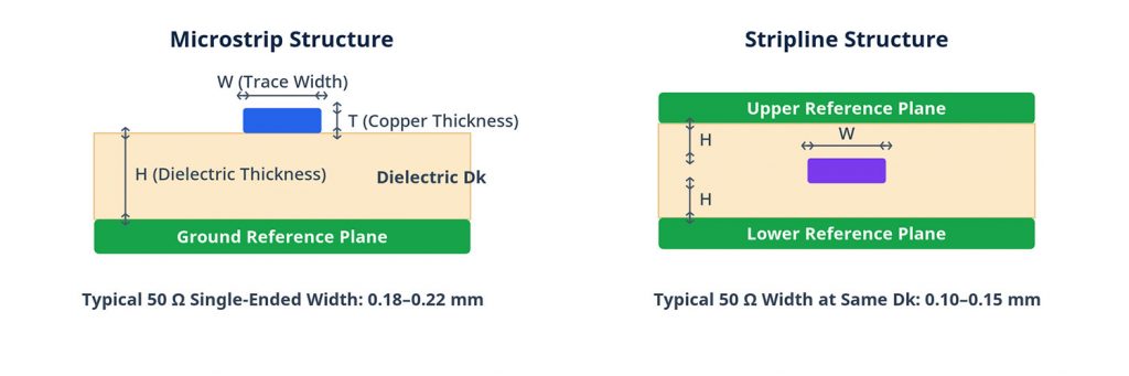
Controlled‑impedance traces are not designed in isolation. The target impedance — 50 Ω single‑ended, 100 Ω differential, or 90 Ω differential for USB — is a function of five parameters that must be consistent with each other and with your fabricator’s actual process data.
The five variables and how they interact
| Variable | Effect on impedance |
|---|---|
| Trace width | Wider → lower impedance |
| Dielectric thickness (h) | Thicker → higher impedance |
| Finished copper thickness (t) | Thicker → slightly lower impedance |
| Dielectric constant (Dk) | Higher Dk → lower impedance |
| Geometry | Microstrip and stripline models differ |
For a microstrip targeting 50 Ω on FR4 (Dk ≈ 4.2–4.5) with 1 oz finished copper and 0.1 mm dielectric to the reference plane, trace width is typically 0.18–0.22 mm. For a buried stripline with the same Dk and 0.1 mm dielectric on each side, the 50 Ω trace width narrows to approximately 0.10–0.15 mm.
Solder mask reduces microstrip impedance by approximately 1–3 Ω depending on mask thickness and coverage. For USB differential pairs targeting 90 Ω, this effect is large enough to matter. Confirm which method your fabricator uses (testing with mask applied versus bare copper) before finalizing trace widths.
Why generic calculators are insufficient
A generic online impedance calculator uses nominal Dk values, nominal copper thickness, and nominal dielectric thickness. Your fabricator works with actual pressed prepreg thickness — which varies by material combination, resin content, and the copper distribution on adjacent inner layers.
Request the fabricator’s stack‑up table and material Dk data, then calculate from those values. If the fabricator offers impedance test coupons on the panel, include them in the build specification. Final trace‑width compensation — the etching adjustment that ensures a 0.20 mm drawn trace produces a 0.20 mm finished trace — should be confirmed in writing before the files are released to production.
Core and Prepreg: What Controls the Final Pressed Thickness
A multilayer PCB is built from alternating rigid cores — copper‑clad laminates already cured — and prepreg sheets, uncured B‑stage glass‑epoxy that flows and bonds during lamination. The distinction matters because the final pressed thickness of a prepreg layer is not the same as its nominal thickness.
During lamination, prepreg resin flows into gaps left by the copper pattern on adjacent inner layers. A layer with 70% copper coverage allows less resin flow than a layer with 30% coverage. The actual dielectric thickness after pressing therefore depends on the inner‑layer copper distribution — not just the prepreg part number.
For impedance‑controlled inner‑layer traces, this variation directly affects impedance. Uneven copper density across a layer produces uneven dielectric thickness across the panel. In practice:
- A 7628 prepreg (high glass content, low resin) flows less during lamination and compresses less
- A 1080 or 106 prepreg (low glass content, high resin) flows more and is preferred when a thin, controlled dielectric is needed
- Core thickness is fixed — cores are pre‑cured and do not compress during lamination
When your impedance target requires a specific dielectric thickness, confirm with the fabricator which prepreg combination achieves that thickness after pressing with your inner‑layer copper distribution — not which nominal prepreg thickness matches the number.
Copper Weight Decisions by Layer
Copper weight affects impedance, minimum achievable line width and spacing, current‑carrying capacity, via barrel plating, and thermal performance. The choice is not simply 0.5 oz inner and 1 oz outer — it depends on what the layer is doing.
Inner layers
Common inner‑layer copper weights are 0.5 oz (17 µm) and 1 oz (35 µm). Heavier inner copper raises the minimum achievable trace width and spacing. Typical minimums are 0.10 mm trace and space for 0.5 oz inner copper, versus 0.15 mm for 1 oz inner copper, depending on fabricator capability. For fine‑pitch BGA breakout where 0.10 mm traces are required between pads, 0.5 oz inner copper is the correct specification.
When inner layers carry significant current — power planes supplying 5 A or more — 1 oz or 2 oz inner copper may be required. Calculate the required copper cross‑section before specifying copper weight, and confirm that the heavier copper is compatible with the fabricator’s minimum line width capability for your design.
Outer layers: base copper versus finished copper
Outer layers start as a base copper weight and increase during the plating process. A board specified at 1 oz outer copper typically starts at approximately 0.5 oz base copper, with 0.5 oz added during through‑hole and via electroplating. The finished outer‑layer copper is approximately 1 oz (35 µm), but the copper in via barrels is the plating thickness only — approximately 20–25 µm. IPC‑6012 Class 2 requires a minimum of 20 µm in the via barrel; Class 3 requires 25 µm.
The finished copper thickness after plating — not the base copper specification — is what enters the impedance calculation. Confirm the expected finished copper thickness with your fabricator before finalizing outer‑layer trace widths.
Fabrication note: Specifying 2 oz outer copper increases manufacturing complexity. The etch factor changes, minimum trace width and spacing increase, and isolated fine features are at higher risk of overetching. For high‑current applications on outer layers, using wider traces at 1 oz finished copper is often preferable to moving to 2 oz.
Working with Your Fabricator: Standard Versus Custom Stack‑Ups
The clearest way to avoid stack‑up rework is to start from the fabricator’s standard material construction and adjust trace geometry to meet impedance targets — not design impedance traces first and then ask the fabricator to match a custom dielectric thickness.
What the fabricator can adjust without re‑approval
During DFM review, fabricators regularly propose minor adjustments that do not require layout changes:
- Core or prepreg combination within the same nominal thickness range
- Actual pressed dielectric thickness within tolerance
- Trace‑width compensation to account for etching
- Base copper selection within an approved finished‑copper specification
- Material substitution within the same Dk and Df performance class
These are process‑level decisions. They are acceptable provided the impedance tolerance remains within ±10% and no signal layer is repositioned relative to its reference plane.
What requires design team sign‑off
The following must not change without explicit approval from the design team:
- Layer count
- Layer function (converting a signal layer to a plane, or vice versa)
- Reference‑plane assignment for any impedance‑controlled layer
- Target impedance value
- Finished copper thickness on layers with current‑carrying requirements
- Material specification for high‑Tg, high‑frequency, or halogen‑free applications
For mixed‑material constructions — a hybrid stack combining standard FR4 cores with high‑frequency PTFE or ceramic‑filled prepreg for RF sections — any material substitution is a design change, not a DFM adjustment.
Design scenario: 6‑layer board for a 2.4 GHz RF front‑end
Consider a 6‑layer design for a 2.4 GHz RF front‑end module with an integrated MCU and power management. The design carries two RF traces requiring 50 Ω microstrip, a USB 2.0 differential pair targeting 90 Ω, three power rails (3.3 V, 1.8 V, 1.2 V), and a 120 MHz MCU clock.
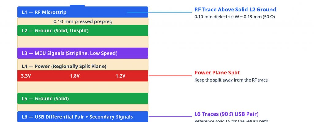
Layer assignment:
| Layer | Function | Reasoning |
|---|---|---|
| L1 | RF signal, microstrip | Short traces above continuous L2 ground |
| L2 | Ground (continuous, uninterrupted) | Reference for L1 RF and L3 |
| L3 | MCU signal, low‑speed routing | Buried stripline, referenced to L2 and L4 |
| L4 | Power (split: 3.3 V / 1.8 V / 1.2 V) | Isolated by function area, no splits under RF traces |
| L5 | Ground (continuous) | Reference for L6 USB traces |
| L6 | USB differential pair + secondary signals | Referenced to L5 |
The L1–L2 dielectric must be thin enough to achieve 50 Ω with a manufacturable trace width. With FR4 Dk ≈ 4.3 and 1 oz finished outer copper, a 0.10 mm pressed dielectric between L1 and L2 gives approximately 0.19 mm trace width for 50 Ω microstrip — within standard fabrication capability. The engineer should confirm:
- Which prepreg combination achieves 0.10 ± 0.01 mm between L1 and L2 after pressing with the actual inner‑layer copper distribution
- Whether trace‑width compensation is applied before or after the impedance calculation
- Whether 50 Ω and 90 Ω test coupons can appear on the same panel
A 4‑layer version is not viable. Combining RF traces, USB differential pairs, and three split power planes in four layers requires at least one signal layer to run without a solid reference plane. That configuration fails EMI pre‑compliance for the RF section.
Decision Sequence Before You Route
Make stack‑up decisions in this order:
- Determine layer count based on routing density, BGA fanout, power rail count, and EMI requirements
- Assign layer functions and confirm every high‑speed signal layer has an adjacent, continuous reference plane
- Identify controlled‑impedance layers and target geometries — microstrip or stripline, single‑ended or differential
- Request the fabricator’s standard stack‑up table and calculate trace widths from actual material data, not nominal values
- Confirm copper weight per layer based on current requirements, minimum line width, and via plating specifications
- Lock the construction and define which parameters require design‑team sign‑off before the fabricator proposes adjustments
Changes made before routing cost nothing. Changes made after routing is closed often require partial or full re‑layout.