The surface finish on a PCB pad does two things: it protects the copper from oxidation during storage and gives solder something to wet to during assembly. ENIG and HASL are the two most common finishes, and the choice between them affects solder joint reliability, component compatibility, and unit cost. This article explains the technical differences and gives you a clear framework for deciding which finish fits your board.
Table of Contents
What ENIG and HASL Surface Finishes Actually Do
HASL (Hot Air Solder Leveling) dips bare copper pads into a molten solder bath, then uses hot air knives to blow off the excess, leaving a thin solder coating on the pad surface. ENIG (Electroless Nickel Immersion Gold) deposits a nickel layer first, then a thin gold layer on top — no heat, no mechanical leveling, pure chemistry.
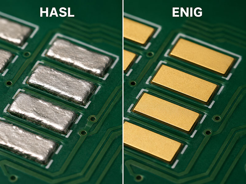
The process difference has one consequence that drives most of the selection logic: surface flatness.
HASL’s air-leveling step cannot produce a perfectly co-planar pad. Solder deposit thickness varies across a board — leaded HASL typically runs 10–25 µm variation, while lead-free HASL runs 15–40 µm due to its higher alloy surface tension. On smaller pads the surface tends to be convex. ENIG’s chemical deposition is uniform — pad-to-pad variation is typically within ±2–3 µm. That difference is irrelevant for a through-hole connector. For a 0.4 mm pitch BGA with 200 balls, it determines whether paste deposits are consistent enough to avoid bridging and opens.
The layer structure of ENIG also matters for understanding its behavior during reflow. The nickel layer — deposited at 3–6 µm per IPC-4552 — acts as a diffusion barrier between copper and the solder joint. The gold layer (0.075–0.125 µm typical) protects the nickel from oxidizing before assembly. During reflow, the gold dissolves rapidly into the solder joint and the bond forms at the nickel interface. This is why ENIG pads can survive multiple reflow cycles without the pad surface degrading.
ENIG vs HASL: Key Differences
The choice between ENIG and HASL comes down to five parameters. Each one maps to a real decision the engineer or procurement manager needs to make.
| Parameter | HASL (Leaded) | Lead-Free HASL | ENIG |
|---|---|---|---|
| Surface flatness | 10–25 µm variation | 15–40 µm variation | ±2–3 µm, co-planar |
| Minimum pitch (reliable yield) | ≥0.8 mm | ≥0.65–0.8 mm* | ≥0.3 mm (BGA/QFN compatible) |
| Shelf life | 6–12 months | 6–12 months | 12+ months |
| Reflow cycles (reliable) | 1–2 passes | 1–2 passes | 3+ passes |
| Cost (relative to ENIG) | Lower | Lower (narrower gap) | Baseline |
* 0.65–0.8 mm is an industry experience value for acceptable yield, not an IPC-defined specification limit.
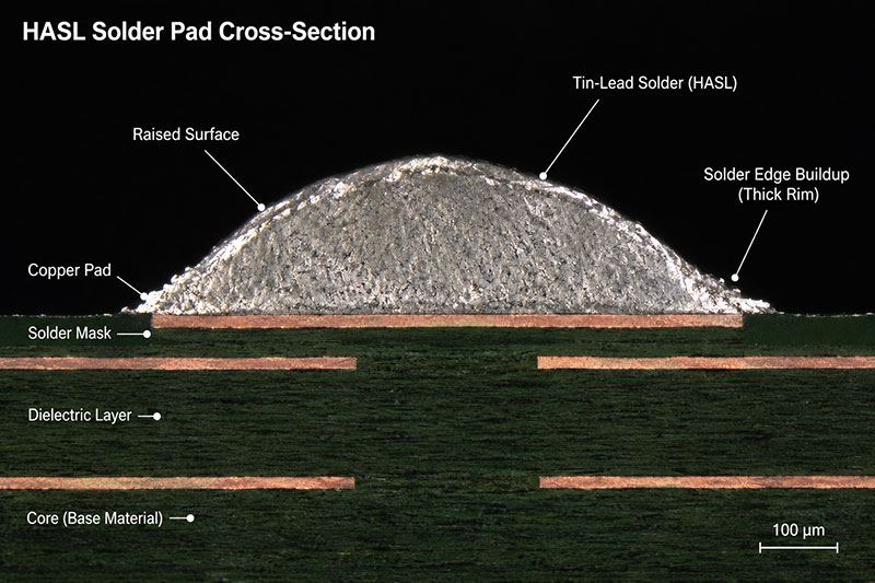
Surface flatness is the clearest differentiator between the two processes. HASL’s uneven surface is manageable at 0.8 mm pitch and above. Below that, the variation in solder height causes inconsistent paste volume and increases the risk of solder bridging or insufficient joints. ENIG’s co-planar surface is why it became the default for BGAs, QFNs, and any fine-pitch IC package.
Shelf life is often underestimated at the design stage. HASL pads — leaded or lead-free — begin oxidizing from the moment the solder surface is exposed to air. Under normal warehouse storage, solderability can degrade within 6–12 months. ENIG’s gold layer resists oxidation and maintains reliable solderability for 12 months or longer. For boards manufactured in advance and assembled in batches, ENIG reduces scrap risk from oxidized pads.
Reflow cycles matter when a board goes through secondary soldering, selective soldering after wave, or field rework. Each thermal pass thins the HASL deposit on smaller pads. After two passes, HASL-finished pads on fine-pitch components may have insufficient solder for a reliable joint. The nickel layer in ENIG does not degrade in the same way, making it the more suitable finish for boards that will see multiple heat exposures.
Lead-Free HASL vs ENIG for RoHS Projects
Leaded HASL is no longer the baseline for most PCB projects. Under RoHS compliance, the real comparison today is Lead-Free HASL against ENIG — and the difference is smaller than buyers sometimes expect.
LF HASL uses SnAgCu (SAC305) or SnCu alloys instead of traditional SnPb. The process still uses hot-air leveling, but at higher temperatures — SAC305 requires a processing bath above 217°C, with board-level peak temperatures of 245–260°C, compared to 183°C for eutectic SnPb. This higher processing temperature increases thermal stress on the board during fabrication, which can be relevant for thin or multilayer boards with fine features.
The flatness problem is not resolved by switching to lead-free alloys. Lead-free HASL does not produce a meaningfully flatter surface than leaded HASL — SAC alloys have higher surface tension than SnPb, and thickness variation on LF HASL boards (15–40 µm) is comparable to or greater than leaded HASL (10–25 µm). For designs with minimum pad pitch at or above 0.8 mm, LF HASL remains a workable choice. For any board with components below 0.65 mm pitch, the flatness gap between LF HASL and ENIG is still a real yield risk.
The cost gap between LF HASL and ENIG has also narrowed. Lead-free alloys cost more than SnPb, so the price premium for choosing ENIG over LF HASL is smaller than the old leaded-HASL-versus-ENIG comparison. On a typical 2-layer board, LF HASL still comes in lower — but sometimes by only 10–15% on the surface finish line item, not the 30–40% gap some buyers assume.
LF HASL is appropriate for: boards with 0.8 mm pitch or coarser, through-hole dominant designs, single-sided boards, short shelf life requirements (assembled within 3–6 months of fabrication), and cost-sensitive prototyping runs.
LF HASL is a poor fit for: BGAs, QFNs, or any component below 0.65 mm pitch; boards requiring three or more reflow cycles; assemblies where shelf life exceeds 6 months; and medical, automotive, or other designs where IPC Class 3 acceptance criteria apply.
ENIG vs HASL Cost and Reliability Trade-Offs
Why ENIG Costs More
ENIG is more expensive than HASL for three reasons: chemical bath complexity, gold material cost, and tighter process controls. The nickel and gold deposition chemistry requires careful bath management to hold deposition rates and layer thickness within IPC-4552 tolerances. Gold is a real material cost even at the thin layers used. Fabricators must monitor and control the process closely to avoid black pad — the main ENIG failure mode.
On a typical 4-layer board in low-to-medium volume, ENIG adds 20–40% to the surface finish cost compared to LF HASL. At the unit price level, the absolute premium depends on board size and pad density. For small boards with few pads, the cost increase is modest. For large, pad-dense boards, it scales with pad area.
For procurement: when comparing ENIG quotes across fabricators, confirm whether the pricing reflects IPC-4552 specifications for nickel and gold thickness. Some lower-cost ENIG processes use gold below 0.05 µm. Thinner gold reduces deposition cost but shortens usable shelf life and increases the risk of poor wetting at assembly.
ENIG Reliability: The Black Pad Risk
ENIG’s primary failure mode is black pad — nickel corrosion that occurs during the immersion gold step when the gold chemistry attacks the nickel surface too aggressively. The result is a phosphorus-rich, brittle nickel interface under the gold layer. When solder reflows onto a black pad, the joint may appear normal during visual or even AOI inspection, but it has significantly reduced shear strength. Failures typically appear as pad-level fractures under mechanical stress — board flexion, drop testing, or connector insertion.
Black pad is not caused by ENIG as a process; it is caused by poor bath control or aggressive chemistry at the fabricator. Selecting a fabricator that documents IPC-4552 compliance and performs regular bath monitoring substantially reduces the risk. For high-reliability or IPC Class 3 applications, requesting cross-section inspection on a sample lot provides direct confirmation of Ni and Au layer quality.
HASL Reliability: Thermal and Storage Limits
HASL’s reliability concerns are different in character. Repeated thermal cycling thins the solder deposit on smaller pads — after two or more reflow passes, HASL-finished fine-pitch pads may carry insufficient solder volume. This rarely matters for through-hole boards assembled in a single pass, but it is relevant for boards designed for rework or secondary soldering operations.
Storage is the other constraint. HASL pads begin oxidizing from the moment solder contacts air. Under standard conditions, most HASL boards should be assembled within 6–12 months of fabrication. Beyond that window, solderability testing before assembly is advisable. ENIG’s gold surface resists oxidation reliably for 12 months and often longer — a meaningful difference for boards that sit in inventory before going to assembly.
How to Choose Between ENIG and HASL
The decision comes down to four variables: component pitch, reflow cycle count, storage duration, and application reliability class.
Choose ENIG when:
- Your design includes any BGA, QFN, or component with pad pitch below 0.5 mm — surface flatness makes this non-negotiable regardless of cost
- The board requires three or more reflow cycles, or field rework is expected
- Shelf life before assembly exceeds 12 months
- The application requires IPC Class 3 acceptance (medical, automotive, aerospace, industrial safety)
- The design mixes fine-pitch SMT and through-hole components — ENIG handles all pad types in a single finish
Choose LF HASL when:
- Minimum component pitch is 0.8 mm or coarser
- The board is through-hole dominant or uses only standard SMT packages (0402, SOT, DIP, SOP with ≥0.65 mm pitch)
- Assembly happens within 6 months of fabrication
- The application does not require IPC Class 3 and cost is the primary constraint
- The design is for prototyping or early engineering builds where absolute yield is less critical than unit cost
If the board has any BGA or sub-0.65 mm pitch component, the surface flatness requirement alone decides the question. ENIG is the right finish. The cost premium is real but smaller than the cost of a yield loss or rework cycle from pad co-planarity issues.
For boards between 0.65 and 0.8 mm pitch with no BGA — assembled within 6 months — LF HASL is viable. If yield consistency matters more than unit cost, ENIG is the lower-risk choice. That trade-off is worth making explicit when placing the order, not discovering it during first article inspection.